Table of Contents
Advertisement
Quick Links
Advertisement
Table of Contents

Related Manuals for Advantech ALDER LAKE-N


Summary of Contents for Advantech ALDER LAKE-N
- Page 2 Manual Advantech MIO-5154 3.5" SBC with Intel® Core™ i3-N305, N-series N97 and N50 Alder Lake N processor The information contained in this document has been carefully researched and is, to the best of our knowledge, accurate. However, we assume no liability for any product failures or damages, immediate or consequential, resulting from the use of the information provided herein.
- Page 3 User Manual MIO-5154 Intel® Core™ i3-N305 Processor, Intel® Processor N-series 3.5" SBC (Code name: Alder Lake N)
- Page 4 No part of this manual may be reproduced, copied, translated, or transmitted in any form or by any means without the prior written permission of Advantech Co., Ltd. The information provided in this manual is intended to be accurate and reliable.
- Page 5 Product Warranty (2 Years) Advantech warrants the original purchaser that each of its products will be free from defects in materials and workmanship for two years from the date of purchase. This warranty does not apply to any products that have been repaired or altered by persons other than repair personnel authorized by Advantech, or products that have been subject to misuse, abuse, accident, or improper installation.
- Page 6 Discard used batteries according to the manufacturer's instructions. Technical Support and Assistance Visit the Advantech web site at www.advantech.com/support where you can find the latest information about the product. Contact your distributor, sales representative, or Advantech's customer service center for technical support if you need additional assistance. Please have the following information ready before you call: –...
- Page 7 Packing List Before you begin installing your card, please make sure that the following materials have been shipped: 1 x MIO-5154 SBC 1 x SATA Cable 30cm (p/n: 1700006291) 1 x SATA Power Cable 35cm (p/n: 1700031583-01) 1 x USB 3.0 Cable 35cm (p/n: 1700032181-01) ...
- Page 8 MIO-5154 User Manual...
-
Page 9: Table Of Contents
Contents Chapter General Information ......1 Introduction ....................2 Specifications .................... 2 Table 1.1: Specifications ............. 2 Block Diagram................... 4 Figure 1.1 Block Diagram ............4 Chapter Mechanical ...........5 Board Layout: Dimensions ................ 6 Figure 2.1 MIO-5154 Mechanical Drawing (Top Side) ....6 Figure 2.2 MIO-5154 Mechanical Drawing (Bottom Side) ... - Page 10 Table 3.14:COM Port Connector (RS232) ......... 17 3.4.13 COM Port Connector (RS232)............ 17 Table 3.15:COM Port Connector (RS232) ......... 18 3.4.14 Audio Connector ................. 18 Table 3.16:Audio Connector............18 3.4.15 LVDS Connector................. 19 Table 3.17:LVDS Connector ............19 3.4.16 SMB Connector ................20 Table 3.18:SMB Connector ............
- Page 11 Figure 4.24.................. 49 Figure 4.25.................. 49 Figure 4.26.................. 50 Figure 4.27.................. 51 Figure 4.28.................. 52 Figure 4.29.................. 53 Figure 4.30.................. 53 4.1.4 Chipset Configuration ..............54 Figure 4.31.................. 54 Figure 4.32.................. 55 Figure 4.33.................. 56 Figure 4.34.................. 57 Figure 4.35.................. 58 Figure 4.36..................
- Page 12 MIO-5154 User Manual...
-
Page 13: Chapter 1 General Information
Chapter General Information This chapter gives background information on the MIO-5154. Sections include: Introduction Specifications Block Diagram... -
Page 14: Introduction
Intel® Core™ i3-N305 and Intel® Processor N-Series processors. MIO-5154 offers embedded iManager 3.0, SUSI 4.0, and WISE-DeviceOn created by Advantech to monitor and control system operation effectively and remotely. MIO-5154 supports single-channel DDR5-4800 up to 16GB, three independent dis- plays via LVDS, DP 1.4, and HDMI 2.0 up to 4K@60Hz, Dual GbE, 6 x USB, 6 x... - Page 15 Table 1.1: Specifications SATA 1 x SATA Gen III, 6.0 Gbps USB 3.0 Serial Bus I2C (Optional to SMBus) COM Port 2 x RS-232/422/485, 4 x RS-232 GPIO 8-bit general purpose input output I/O Internal I/O Audio Realtek ALC888s, Line-in/Line-out/Mic Inverter 5V @2A Smart Fan...
-
Page 16: Block Diagram
Block Diagram Figure 1.1 Block Diagram MIO-5154 User Manual... -
Page 17: Chapter 2 Mechanical
Chapter Mechanical This chapter gives mechanical information on the MIO-5154. Sections include: Mechanical Drawing Assembly Drawing... -
Page 18: Board Layout: Dimensions
This chapter includes board dimensions and the standard thermal solution. Board Layout: Dimensions 102.0 98.7 92.7 82.5 31.5 27.2 20.5 Figure 2.1 MIO-5154 Mechanical Drawing (Top Side) 102.0 98.7 92.7 92.3 73.3 27.2 20.5 17.9 Figure 2.2 MIO-5154 Mechanical Drawing (Bottom Side) MIO-5154 User Manual... - Page 19 10.8 Figure 2.3 MIO-5154 Mechanical Drawing (Coastline) 102.0 98.7 92.7 82.5 31.5 27.2 20.5 Figure 2.4 MIO-5154 Mechanical Drawing with CPU Heatsink (Top Side) MIO-5154 User Manual...
-
Page 20: (Coastline)
24.0 10.8 Figure 2.5 MIO-5154 Mechanical Drawing with 15W/12W CPU Heatsink (Coastline) 16.2 14.6 10.8 Figure 2.6 MIO-5154 Mechanical Drawing with 6W CPU Heatsink (Coastline) MIO-5154 User Manual... -
Page 21: Chapter 3 Installation
Chapter Installation This chapter explains the setup procedures of the MIO-5154 hard- ware, including instructions on setting jumpers and connecting peripherals, switches, and indica- tors. Be sure to read all safety pre- cautions before you begin the installation procedure. -
Page 22: Jumpers & Switches
Jumpers & Switches The MIO-5154 has a number of jumpers that allow you to configure your system to suit your application. The table below lists the functions of the various jumpers. Table 3.1: Jumpers & Switches JCMOS1 CMOS Clear Switch VDD1 Panel Voltage Selection RI_VDD1... -
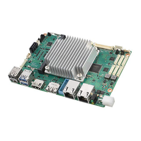
Page 23: Locating Connectors
Locating Connectors JCMOS1 VDD1 AT_ATX1 DIMMA1 GPIO1 LVDS1 FAN1 RI_VDD1 AUDIO1 COM2 COM3 SATAP1 COM5 SATA1 COM1 COM4 COM6 I2C_SMB1 DCIN1/2 LAN1 LAN2 USB2_1 USB3_1 HDMI1 USB1 Figure 3.1 MIO-5154 Connector Locations (Top Side) M2_B1 M2_E1 SIM1 M2_B2 BAT1 Figure 3.2 MIO-5154 Connector Locations (Bottom Side) MIO-5154 User Manual... -
Page 24: Setting Jumpers
Setting Jumpers You may configure your card to match the needs of your application by setting jump- ers. A jumper is a metal bridge used to close an electric circuit. It consists of two metal pins and a small metal clip (often protected by a plastic cover) that slides over the pins to connect them. -
Page 25: Panel Voltage Selection (Vdd1)
3.4.2 Panel Voltage Selection (VDD1) Table 3.4: Panel Voltage Selection Function Jumper Setting Panel Voltage Setting: +V3.3 (Default) Panel Voltage Setting: +V5 Panel Voltage Setting: +V12 Signal Pin Definition +V3.3 +V_LVDS_LCD +V12 3.4.3 COM RI# pin 5V/12V Selection (RI_VDD1) Table 3.5: COM RI# pin 5V/12V Selection Function Jumper Setting RI# Voltage Setting: +V5... -
Page 26: Atx/At Mode Selection
Signal Pin Definition VCCAT PU to 3.3V suspend VCCATX 3.4.4 ATX/AT Mode Selection Table 3.6: ATX/AT Mode Selection Function Jumper Setting BIOS setting to AT mode (Default) BIOS setting to ATX mode Signal Pin Definition VCCAT PU to 3.3V suspend VCCATX 3.4.5 DC Input Connector... -
Page 27: Internal Usb 3.1 Gen1 Connector
3.4.7 Internal USB 3.1 Gen1 Connector Table 3.9: Internal USB 3.1 Gen1 Connector Signal Pin Definition Vbus IntA_P1_SSRX- IntA_P1_SSRX+ IntA_P1_SSTX- IntA_P1_SSTX+ IntA_P1_D- IntA_P1_D+ IntA_P2_D+ IntA_P2_D- IntA_P2_SSTX+ IntA_P2_SSTX- IntA_P2_SSRX+ IntA_P2_SSRX- Vbus No Pin 3.4.8 COM Port Connector (RS232+RS422+RS485) Table 3.10: COM Port Connector (RS232+RS422+RS485) Signal Pin Definition COM1_z_RI# COM1_DTR#... -
Page 28: Com Port Connector (Rs232+Rs422+Rs485)
Table 3.10: COM Port Connector (RS232+RS422+RS485) COM1_DCD# 3.4.9 COM Port Connector (RS232+RS422+RS485) Table 3.11: COM Port Connector (RS232+RS422+RS485) Signal Pin Definition COM2_RI# COM2_DTR# COM2_CTS# COM2_TXD COM2_RTS# COM2_RXD COM2_DSR# COM2_DCD# 3.4.10 COM Port Connector (RS232) Table 3.12: COM Port Connector (RS232) Signal Pin Definition COM3_RI# COM3_DTR#... -
Page 29: Com Port Connector (Rs232)
3.4.11 COM Port Connector (RS232) Table 3.13: COM Port Connector (RS232) Signal Pin Definition COM4_RI# COM4_DTR# COM4_CTS# COM4_SOUT COM4_RTS# COM4_SIN COM4_DSR# COM4_DCD# 3.4.12 COM Port Connector (RS232) Table 3.14: COM Port Connector (RS232) Signal Pin Definition COM5_RI# COM5_DTR# COM5_CTS# COM5_SOUT COM5_RTS# COM5_SIN COM5_DSR#... -
Page 30: Audio Connector
Table 3.15: COM Port Connector (RS232) Signal Pin Definition COM6_RI# COM6_DTR# COM6_CTS# COM6_SOUT COM6_RTS# COM6_SIN COM6_DSR# COM6_DCD# 3.4.14 Audio Connector Table 3.16: Audio Connector Signal Pin Definition LOUTR LINR LOUTL LINL MIC1R MIC1L MIO-5154 User Manual... -
Page 31: Lvds Connector
3.4.15 LVDS Connector Table 3.17: LVDS Connector Signal Pin Definition +V_LCD +V_LCD +V_LCD +V_LCD LVDS1_0_D0- LVDS1_1_D0- LVDS1_0_D0+ LVDS1_1_D0+ LVDS1_0_D1- LVDS1_1_D1- LVDS1_0_D1+ LVDS1_1_D1+ LVDS1_0_D2- LVDS1_1_D2- LVDS1_0_D2+ LVDS1_1_D2+ LVDS1_0_CLK- LVDS1_1_CLK- LVDS1_0_CLK+ MIO-5154 User Manual... -
Page 32: Smb Connector
Table 3.17: LVDS Connector LVDS1_1_CLK+ LVDS0_DDCCLK_AUX+ LVDS0_DDCDAT_AUX- LVDS1_0_D3- LVDS1_1_D3- LVDS1_0_D3+ LVDS1_1_D3+ LVDS1_VCON 3.4.16 SMB Connector Table 3.18: SMB Connector Signal Pin Definition EC_SMB0_z_DAT EC_SMB0_z_CLK +V3.3_DUAL 3.4.17 Fan Connector Table 3.19: Fan Connector Signal Pin Definition +V12 FAN_SPEED FAN_V5_PWM MIO-5154 User Manual... -
Page 33: Sata Power Connector
3.4.18 SATA Power Connector Table 3.20: SATA Power Connector Signal Pin Definition 3.4.19 Panel Inverter Connector Table 3.21: Panel Inverter Connector Signal Pin Definition +V12_1_INVERTER_0 LVDS1_Z_ENABKL EC_LVDS1_Z_PWM +V5_1_INVERTER_0 3.4.20 GPIO Connector Table 3.22: GPIO Connector Signal Pin Definition SIO_GPIO7 SIO_GPIO2 SIO_GPIO6 SIO_GPIO1 SIO_GPIO5... -
Page 34: Power / Led / Case Open / Buzzer Connector
3.4.21 Power / LED / Case Open / Buzzer Connector Table 3.23: Power / LED / Case Open / Buzzer Connector Signal Pin Definition BUZZER- BUZZER+ RDC_CASEOPEN SATA_EXT_LED# FP_A_PSIN# FP_A_RST# +3.3V 3.4.22 M.2 B-Key (PCIe x1 / USB 2.0) Table 3.24: M.2 B-Key (PCIe x1 / USB 2.0) Signal Pin Definition Signal Pin Definition 3.3V (Suspend) -
Page 35: B-Key (Sata / Pcie X1)
Table 3.24: M.2 B-Key (PCIe x1 / USB 2.0) PETn0 UIM_PWR USB3.1-Rx+ UIM_DATA USB3.1-Rx- UIM_CLK UIM_RESET USB3.1-Tx+ USB3.1-Tx- CONFIG_0 (Pull up 10K to 3.3V) M2B1_SATA_DEVSLP_R M2B1_SATA_DEVSLP_R LED_1# (3.3V) W_DISABLE1# (3.3V) USB_D- FULL_CARD_POW- USB_D+ ER_OFF# (1.8V) 3.3V (Suspend) 3.3V (Suspend) CONFIG_3 (Pull up 10K to 3.3V) 3.4.23 M.2 B-Key (SATA / PCIe x1) Table 3.25: M.2 B-Key (SATA / PCIe x1) -
Page 36: E-Key (Pcie X1 / Usb 2.0)
Table 3.25: M.2 B-Key (SATA / PCIe x1) PERp0 / SATA-A+ PERn0 / SATA-A- PETp0 / SATA-B- PETn0 / SATA-B+ CONFIG_0 (Pull up 10K to 3.3V) M2B1_SATA_DEVSLP_R M2B1_SATA_DEVSLP_R LED_1# (3.3V) W_DISABLE1# (3.3V) FULL_CARD_POW- ER_OFF# (1.8V) 3.3V (Suspend) 3.3V (Suspend) CONFIG_3 (Pull up 10K to 3.3V) 3.4.24 M.2 E-Key (PCIe x1 / USB 2.0) Table 3.26: M.2 E-Key (PCIe x1 / USB 2.0) -
Page 37: Rtc Battery Connector
Table 3.26: M.2 E-Key (PCIe x1 / USB 2.0) W_DISABLE1# (3.3V) W_DISABLE2# (3.3V) PEWAKE0# (3.3V) PERST0# (3.3V) CLKREQ0# (3.3V) SUSCLK (3.3V) REFCLKn0 REFCLKp0 PETn0 PETp0 PERn0 PERp0 M2B1_SATA_DEVSLP_R 30 M2B1_SATA_DEVSLP_R 3.3V (Suspend) USB_D- 3.3V (Suspend) USB_D+ 3.4.25 RTC Battery Connector Table 3.27: RTC Battery Connector Signal Pin Definition +VBAT_b1... -
Page 38: Nano Sim Connector
3.4.26 Nano SIM Connector Table 3.28: Nano SIM Connector Signal Pin Definition RESET Clock Data MIO-5154 User Manual... -
Page 39: Ami Bios Setup
Chapter AMI BIOS Setup... -
Page 40: Entering Setup
BIOS supports your CPU. If there is no number assigned to the patch code, please contact an Advantech application engineer to obtain an up-to-date patch code file. This will ensure that your CPU‘s system status is valid. -
Page 41: Main Setup
4.1.1 Main Setup When you first enter the BIOS Setup Utility, you will encounter the Main setup screen. You can always return to the Main setup screen by selecting the Main tab. There are two Main Setup options. They are described in this section. The Main BIOS Setup screen is shown below. -
Page 42: Advanced Bios Features Setup
4.1.2 Advanced BIOS Features Setup Select the Advanced tab from the MIO-5154 setup screen to enter the Advanced BIOS Setup screen. You can select any of the items in the left frame of the screen, such as CPU Configuration, to go to the sub-menu for that item. You can display an Advanced BIOS Setup option by highlighting it using the <Arrow>... -
Page 43: Rc Acpi Settings
4.1.3 RC ACPI Settings Figure 4.4 PTID Support Enable/Disable to load the PTID Table. Native PCIE Enable Enable/Disable PCIE Native Control reported in the ACPI Table. Native ASPM Choose if the ASPM feature is controlled by the OS or BIOS. BDAT ACPI Table Support ... - Page 44 4.1.3.1 WWAN Configuration Figure 4.5 WWAN Device Select the M.2 WWAN Device options to enable 5G-M80 (MediaTek) Modems. 4.1.3.2 CPU Configuration Figure 4.6 MIO-5154 User Manual...
- Page 45 C6DRAM Enable/Disable moving of DRAM contents to PRM memory when the CPU is in C6 state. CPU Flex Ratio Override Enable/Disable CPU Flex Ratio Programming. Hardware Prefetcher This item allows users to enable or disable the hardware prefetcher feature. Adjacent Cache Line Prefetch ...
- Page 46 CPU – Power Management Control CPU – Power Management Control Options. GT – Power Management Control GT – Power Management Control Options. CPU - Power Management Control Figure 4.8 Boot Performance mode Select the performance state that the BIOS will set before OS handoff. Intel®...
- Page 47 Enable/Disable CPU Power Management. PowerLimit 3 Settings Power Limit 3 Settings. View/Configure Turbo Options Figure 4.9 Turbo Ratio Limit Option View/Configure Turbo Ratio Limit Options. Energy Efficient P-state Enable/Disable Energy Efficient P-state feature. Package Power Limit MSR Lock ...
- Page 48 TDP Configurations Figure 4.10 E-core Turbo Ratio Limit Numcore x Efficient-core Turbo Ratio Limit Numcore x defines the core range. Power Limit 3 Settings Figure 4.11 MIO-5154 User Manual...
- Page 49 Power Limit 3 Override Enable/Disable Power Limit 3 override. GT - Power Management Control Figure 4.12 RC6(Render Standby) Check to enable render standby support. Maximum GT frequency Maximum GT frequency limited by user. Disable Turbo GT frequency ...
- Page 50 4.1.3.4 PCH-FW Configuration Figure 4.13 ME State When Disabled, ME will be put ME into Temporarily Disabled Mode. ME Unconfig on RTC Clear When Disabled, ME will not be unconfigured on RTC Clear. Core BIOS Done Message Enable/Disable Core BIOS Done message sent to ME.
- Page 51 4.1.3.5 ACPI Settings Figure 4.14 Enable ACPI Auto Configuration Enable or disable BIOS ACPI auto configuration. Enable Hibernation Enables or Disables the system ability to hibernate (OS/S4 Sleep State). This option may not be effective with some OS. ACPI Sleep State ...
- Page 52 4.1.3.6 NCT6126D Super IO Configuration Figure 4.15 Serial Port 1 Configuration Set Parameters of Serial Port 1. Serial Port 2 Configuration Set Parameters of Serial Port 2. Serial Port 3 Configuration Set Parameters of Serial Port 3. Serial Port 4 Configuration ...
- Page 53 Serial Port 1 Configuration Figure 4.16 Serial Port Enable or Disable Serial Port (COM). Change Settings Select an optimal settings for a Super IO device. COM Port Mode COM Port Mode Select. MIO-5154 User Manual...
- Page 54 Serial Port 2 Configuration Figure 4.17 Serial Port Enable or Disable Serial Port (COM). Change Settings Select an optimal setting for a Super IO device. COM Port Mode COM Port Mode Select. MIO-5154 User Manual...
- Page 55 Serial Port 3 Configuration Figure 4.18 Serial Port Enable or Disable Serial Port (COM). Change Settings Select optimal settings for a Super IO device. MIO-5154 User Manual...
- Page 56 Serial Port 4 Configuration Figure 4.19 Serial Port Enable or Disable Serial Port (COM). Change Settings Select optimal settings for a Super IO device. MIO-5154 User Manual...
- Page 57 Serial Port 5 Configuration Figure 4.20 Serial Port Enable or Disable Serial Port (COM). Change Settings Select optimal settings for a Super IO device. MIO-5154 User Manual...
- Page 58 Serial Port 6 Configuration Figure 4.21 Serial Port Enable or Disable Serial Port (COM). Change Settings Select optimal settings for a Super IO device. MIO-5154 User Manual...
- Page 59 4.1.3.7 NCT6126D HW Monitor Figure 4.22 Smart Fan Function Enable or Disable Smart Fan. Digital I/O Configuration Configure the digital I/O pins. ACPI CPU Shutdown Temperature Select the Critical Temperature value where OSPM must shut down the system. Case Open Detection ...
- Page 60 Smart Fan Function Figure 4.23 System Fan Mode System Fan Mode Select. SYSFAN Temperature 1 Input the System Smart Fan IV Temperature 1. SYSFAN DC/PWM 1 Input the System Smart Fan IV DC/PWM 1 Value. SYSFAN Temperature 2 ...
- Page 61 Digital I/O Configuration Figure 4.24 Digital I/O Pin 1/2/3/4/5/6/7/8 Configure Digital I/O Pins. 4.1.3.8 Trusted Computing Figure 4.25 MIO-5154 User Manual...
- Page 62 TPM Device Selection Select TPM device: fTPM or dTPM. Security Device Support Enable or disable BIOS support for a security device. SHA-1 PCR Bank Enable or Disable SHA-1 PCR Bank. SHA256 PCR Bank Enable or Disable SHA256 PCR Bank. SHA384 PCR Bank ...
- Page 63 Wake system from S5 Enable/Disable System wake-on-alarm event. Select FixedTime for the system to wake at the hr:min:sec specified. 4.1.3.10 Serial Port Console Redirection Figure 4.27 Console Redirection This item allows users to enable or disable console redirection for Microsoft Windows Emergency Management Services (EMS).
- Page 64 4.1.3.11 USB Configuration Figure 4.28 XHCI Hand-off This is a workaround for OS without XHCI hand-off support. The XHCI owner- ship change should be claimed by the XHCI driver. USB Mass Storage Driver Support Enable/Disable USB Mass Storage Driver Support. USB transfer time-out ...
- Page 65 4.1.3.12 Network Stack Configuration Figure 4.29 Network Stack Enable/Disable UEFI Network Stack. 4.1.3.13 NVMe Configuration Figure 4.30 MIO-5154 User Manual...
- Page 66 4.1.4 Chipset Configuration Select the Chipset tab from the MIO-5154 setup screen to enter the Chipset BIOS Setup screen. You can display a Chipset BIOS Setup option by highlighting it using the <Arrow> keys. All Plug and Play BIOS Setup options are described in this sec- tion.
- Page 67 4.1.4.1 System Agent (SA) Configuration Figure 4.32 Memory Configuration Memory Configuration Parameters. Graphics Configuration Graphics Configuration Parameters. DMI/OPI Configuration Control various DMI functions. Display Setup Menu Display Configuration settings. Stop Grant Configuration Automatic/Manual stop grant configuration. VT-d ...
- Page 68 Memory Configuration Figure 4.33 Memory Test on Warm Boot Enable/Disable Base Memory Test Run on Warm Boot. Max TOLUD Maximum Value of TOLUD. SA GV System Agent Geyserville. Gear Ratio Gear ratio when SAGV is disabled. Memory Scrambler ...
- Page 69 Graphics Configuration Figure 4.34 Graphics Turbo IMON Current Graphics turbo IMON current values supported. GTT Size Select the GTT Size. Aperture Size Select the Aperture Size. PSMI Support Enable/Disable PSMI. DVMT Pre-Allocated Select DVMT 5.0 Pre-Allocated (Fixed) Graphics Memory size used by the Internal Graphics Device.
- Page 70 LVDS Figure 4.35 NXP Non-EDID Support Non-EDID Support. Color Depth & Data Packing Color depth and data packing format for Non-EDID Support. Dual LVDS Mode Select LVDS bus to Single bus mode or Dual bus mode. LVDS Panel Type ...
- Page 71 DMI/OPI Configuration Figure 4.36 DMI Gen3 ASPM DMI Gen3 ASPM Support. DMI ASPM DMI ASPM Support. MIO-5154 User Manual...
- Page 72 4.1.4.2 PCH-IO Configuration Figure 4.37 PCI Express Configuration PCI Express Configuration Settings. SATA Configuration SATA Device Options Settings. USB Configuration USB Configuration Settings. Security Configuration Security Configuration Settings. HD Audio Configuration HD Audio Subsystem Configuration Settings. Serial IO Configuration ...
- Page 73 PCI Express Configuration Figure 4.38 DMI Link ASPM Control This item controls Active State Power Management of the DMI Link. PCI Express Root Port 10/12 PCI Express Port 10/12 Settings. MIO-5154 User Manual...
- Page 74 PCI Express Root Port 10 Figure 4.39 PCI Express Root Port 12 Figure 4.40 MIO-5154 User Manual...
- Page 75 SATA Configuration Figure 4.41 SATA Controller(s) Enable/Disable SATA Device. SATA Mode Selection Determine how the SATA controller operates. SATA Controller Speed Limit Indicates the maximum speed the SATA controller can support. Aggressive LPM Support Enable PCH to aggressively enter link power state. MIO-5154 User Manual...
- Page 76 USB Configuration Figure 4.42 USB Overcurrent Select "Enabled" if Overcurrent functionality is used. USB Port Disable Override Selectively Enable/Disable the corresponding USB Port from reporting a device connection to the controller. MIO-5154 User Manual...
- Page 77 Security Configuration Figure 4.43 RTC Memory Lock Enable will lock bytes 38h-3Fh in the lower/upper 128-byte bank of RTC RAM. BIOS Lock Enable or Disable the PCH BIOS Lock Enable feature. Force unlock on all GPIO pads If Enabled, BIOS will force all GPIO pads to be in the unlock state.
- Page 78 HD Audio Configuration Figure 4.44 HD Audio Control Detection of the HD-Audio device. Disabled = HDA will be uncondition- ally disabled. Enabled = HDA will be unconditionally enabled. MIO-5154 User Manual...
- Page 79 Serial IO Configuration Figure 4.45 I2C0 Controller Enable/Disable Serial IO Controller. Serial IO I2C0 Settings Configure Serial IO Controller. MIO-5154 User Manual...
- Page 80 Serial IO I2C0 Settings Figure 4.46 MIO-5154 User Manual...
- Page 81 4.1.5 Security Figure 4.47 Select Security Setup from the MIO-5154 Setup main BIOS setup menu. All Security Setup options, such as password protection and virus protection, are described in this section. To access the sub-menu for the following items, select the item and press <Enter>: Change Administrator / User Password ...
- Page 82 4.1.6 Boot Figure 4.48 Setup Prompt Timeout This is the number of seconds that the firmware will wait before initiating the original default boot selection. A value of 0 indicates that the default boot selec- tion is to be initiated immediately on boot. A value of 65535(0xFFFF) indicates that firmware will wait for user input before booting.
- Page 83 4.1.7 Save & Exit Figure 4.49 Save Changes and Exit This item allows you to exit system setup after saving the changes. Discard Changes and Exit This item allows you to exit system setup without saving any changes. Save Changes and Reset ...
- Page 84 MIO-5154 User Manual...
- Page 85 Appendix System Assignments This appendix contains informa- tion of a detailed nature. Sections include: System I/O Ports 1st MB Memory Map Interrupt Assignments...
- Page 86 System I/O Ports Table A.1: System I/O Ports Addr. Range (Hex) Device 00h-1Fh DMA Controller 20h-2Dh Interrupt Controller 2Eh–2Fh Motherboard resources 30h-3Dh Interrupt Controller 40h-43h Timer/Counter 4Eh–4Fh Motherboard resources 50h-53h Timer/Counter 60h-6Fh 8042 (keyboard controller) / NMI Controller / Microcontroller 70h-7Fh Real-Time Controller 80h-8Fh...
- Page 87 1st MB Memory Map Table A.3: 1st MB Memory Map Addr. Range (Hex) Device E0000h - FFFFFh System board D0000h - DFFFFh PCI Bus C0000h - CFFFFh System board A0000h - BFFFFh PCI Bus A0000h - BFFFFh Intel® HD Graphics 00000h - 9FFFFh System board Interrupt Assignments...
- Page 88 No part of this publication may be reproduced in any form or by any means, electronic, photocopying, recording or otherwise, without prior written permis- sion from the publisher. All brand and product names are trademarks or registered trademarks of their respective companies. © Advantech Co., Ltd. 2024...
- Page 89 Our company network supports you worldwide with offices in Germany, Austria, Switzerland, the UK and the USA. For more information please contact: Headquarters Germany FORTEC Elektronik AG Augsburger Str. 2b 82110 Germering Phone: +49 89 894450-0 E-Mail: info@fortecag.de Internet: www.fortecag.de Fortec Group Members Austria Distec GmbH Office Vienna...
Need help?
Do you have a question about the ALDER LAKE-N and is the answer not in the manual?
Questions and answers