Table of Contents
Advertisement
Quick Links
UM3118
User manual
Motor control Discovery kit with STM32G473QE MCU
Introduction
The
B-G473E-ZEST1S
Discovery kit is a part of the motor-control development platform supporting ZeST and HSO algorithms.
B-G473E-ZEST1S is a control board with STM32G473QET6 microcontroller in ZeST Discovery pack and works together with a
Power board such as STEVAL-LVLP01, an optional adaptor board such as B-ZEST-ADAPT1, and an accessories package such
as B-MOTOR-PMSMA1.
The B-G473E-ZEST1S control board is connected to the power board or adaptor board through an embedded MC connector
V2. B-G473E-ZEST1S can also support motor driver expansion boards X-NUCLEO-IHM08M1, X-NUCLEO-IHM09M1, and X-
NUCLEO-IHM16M1 via the Morpho MC connector. STLINK-V3EC is integrated into the board, as an embedded in-circuit
debugger and programmer for the STM32 MCU and the USB Virtual COM port bridge.
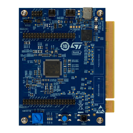
Figure 1.
B-G473E-ZEST1S top view
Figure 2.
B-G473E-ZEST1S bottom view
Pictures are not contractual.
UM3118 - Rev 3 - November 2023
www.st.com
For further information contact your local STMicroelectronics sales office.
Advertisement
Table of Contents

Related Manuals for ST B-G473E-ZEST1S


Summary of Contents for ST B-G473E-ZEST1S
- Page 1 Power board such as STEVAL-LVLP01, an optional adaptor board such as B-ZEST-ADAPT1, and an accessories package such as B-MOTOR-PMSMA1. The B-G473E-ZEST1S control board is connected to the power board or adaptor board through an embedded MC connector V2. B-G473E-ZEST1S can also support motor driver expansion boards X-NUCLEO-IHM08M1, X-NUCLEO-IHM09M1, and X- NUCLEO-IHM16M1 via the Morpho MC connector.
-
Page 2: Features
– Morpho MC – STDC14 and USART debug ports • Flexible power-supply options: 5V from Power board, ST-LINK USB V , or 5V external sources from Morpho MC connector • On-board STLINK-V3EC debugger/programmer with USB re-enumeration capability: two Virtual COM ports, and debug port •... -
Page 3: Ordering Information
UM3118 Ordering information Ordering information To order the B-G473E-ZEST1S Discovery kit, refer to Table 1. Additional information is available from the datasheet and reference manual of the target microcontroller. Table 1. List of available products Order code Board reference Target STM32... -
Page 4: Development Environment
STM32 flash memory for easy demonstration of the device peripherals in standalone mode. The latest versions of the demonstration source code and associated documentation can be downloaded from www.st.com. UM3118 - Rev 3 page 4/38... -
Page 5: Conventions
UM3118 Conventions Conventions Table 3 provides the conventions used for the ON and OFF settings in the present document. Table 3. ON/OFF convention Convention Definition Jumper JPx ON Jumper fitted Jumper JPx OFF Jumper not fitted Jumper JPx [1-2] Jumper fitted between Pin 1 and Pin 2 Solder bridge SBx ON SBx connections closed by 0 Ω... -
Page 6: Quick Start
STLINK-V3EC USB driver available on the www.st.com website. ® Connect the B-G473E-ZEST1S Discovery board to a PC with a USB cable (USB Type-A or USB Type-C ® USB Type-C ) through the STLINK-V3EC USB connector (CN4) to power the board. -
Page 7: Hardware Layout And Configuration
UM3118 Hardware layout and configuration Hardware layout and configuration Hardware block diagram The B-G473E-ZEST1S Discovery board is designed with the STM32G473QET6 target microcontroller. Figure 3 illustrates STM32G473QET6 connections with peripheral components. Figure 4 helps to locate these features on the B-G473E-ZEST1S Discovery board. -
Page 8: Default Board Configuration
UM3118 Default board configuration Figure 4. B-G473E-ZEST1S PCB layout (top view) 5V_PWR USART STLINK-V3EC 5V power connector connector selection STDC14 (LD4) (CN1) (CN2) (CN4) (JP2) STLINK-V3EC Power status LED BOOT0 selection (LD5) (JP1) STLINK-V3EC COM LED (LD6) Morpho MC MC connector V2... -
Page 9: Embedded Stlink-V3Ec
In case the B-G473E-ZEST1S Discovery board is connected to the PC before the driver is installed, some B- G473E-ZEST1S Discovery board interfaces might be declared as Unknown in the PC device manager. In this case, the user must install the dedicated driver files, and update the driver of the connected device from the... -
Page 10: Firmware Upgrade
B-G473E-ZEST1S Discovery board and periodically, to stay up-to-date with the latest firmware version. 6.3.4 Use of an external debugging tool to program and debug the on-board STM32 There are two basic ways to support an external debugging tool: Keep the embedded STLINK-V3EC running. -
Page 11: Table 6. Stdc14/Mipi10 Debug Connector Pinout
UM3118 STDC14/MIPI10 and USART connectors Table 6 describes the STDC14/MIPI10 connector pinout compatible with both interfaces: STDC14 and MIPI10. Table 6. STDC14/MIPI10 debug connector pinout MIPI10 pin STDC14 STM32 pin Board function number pin number Reserved Reserved Target VDD PA13 JTMS_SWDIO: Target SWDIO using the SWD protocol. -
Page 12: Table 8. Usart Debug Connector Pinout
UM3118 STDC14/MIPI10 and USART connectors Figure 7 shows the USART connector (CN1) pinout. Figure 7. USART connector (CN1) pinout Pin 2 Pin 9 Pin 1 Pin 10 Table 8 describes the USART connector pinout. Table 8. USART debug connector pinout Connector pin STM32 pin Board function... -
Page 13: I/O Restriction To Other Features
5 V power supply general view The B-G473E-ZEST1S Discovery board is designed to be powered from the 5 V DC power source. One of the following five 5 V DC power inputs can be used, upon an appropriate board configuration: •... -
Page 14: 5V Stlink-V3Ec Source: 5V_Usb_Stlk
In this case, it is mandatory to power the board first using P5V or E5V then connect the B-G473E-ZEST1S USB cable to the PC. Proceeding this way, the enumeration succeeds thanks to the external power source. -
Page 15: Reset Sources
6.8.1 Description The bootloader is located in the system memory, programmed by ST during production. It is used to reprogram the flash memory via USART, I C, SPI, CAN FD, or USB FS in device mode through the DFU (device firmware upgrade). -
Page 16: Mc Connector V2
MC connector V2 is a new generation interface between the control board and the power board (or adaptor board). It is a PCI Express format connector. On B-G473E-ZEST1S, this connector is a PCI-E 16x edge-finger. Three motors, PFC, SPI, and ADCs signals are implemented on MC connector V2. The signals of the second motor (Motor 2) signals are shared with the Morpho MC signals. - Page 17 UM3118 MC connector V2 STM32 Category Pin name Function of B-G473E-ZEST1S Comment number signal Ph_Voltage+/BEMF_zc PD13 M1_VOL+_W_ADC_345_IN10 Temperature/Board ID PE15 M1_TEMP_ADC_4_IN2 Motor1 VBUS PB13 M1_VBUS_ADC_3_IN5 Dissipative_brake M1_DissipativeBrake(GPIO) DGND AGND AC_voltage M_AC voltage_ADC_2_IN10 M_PFC current PFC_Current1 1_ADC_4_IN12/5_IN12 PFC_BKIN_OC M_PFC_BKIN_OC_TIM_16_BKIN PFC_PWM1 M_PFC_PWM1_TIM_16_CH1...
- Page 18 UM3118 MC connector V2 STM32 Category Pin name Function of B-G473E-ZEST1S Comment number signal Shared with M1_Resolver_Sin/ Shunt+ M3_SHUNT1_ADC_12_IN2 pin B-29 Shared with M1_Resolver_Cos/ Motor3 Shunt+ M3_SHUNT2_ADC_12_IN7 pin B-55 Shared with M2_Resolver_Cos/ Shunt+ M3_SHUNT3_ADC_1_IN3 pin B-30 AGND Ph_Voltage+/BEMF_zc Ph_Voltage+/BEMF_zc Ph_Voltage+/BEMF_zc...
- Page 19 UM3118 MC connector V2 STM32 Category Pin name Function of B-G473E-ZEST1S Comment number signal Shunt- PB10 M1_SHUNT2_OPAMP_4_VINM Motor1 Shunt- PB15 M1_SHUNT3_OPAMP_5_VINM AGND Ph_Voltage-/BEMF_ref Ph_Voltage-/BEMF_ref Ph_Voltage-/BEMF_ref Res.Ex/Curr.REF M1_DAC_1_OUT1 Motor1 M1_Resolver_Sin/ Shared with Resolver_Sin/GPIO_BEMF M3_SHUNT1_ADC_12_IN2 pin A-66 M1_Resolver_Cos/ Shared with Resolver_Cos M3_SHUNT2_ADC_1_IN3...
- Page 20 UM3118 MC connector V2 STM32 Category Pin name Function of B-G473E-ZEST1S Comment number signal M3_EmergencySTOP_TIM_20_BKIN Emergency(BKIN2) PF10 INL/EN M3_PWM_UL_TIM_20_CH1N INL/EN M3_PWM_VL_TIM_20_CH2N INL/EN M3_PWM_WL_TIM_20_CH3N Motor3 Encoder_A Encoder_B Encoder_Z Hall_sensor_H3 DGND Shunt- Motor3 Shunt- Shunt- AGND Ph_Voltage-/BEMF_ref Ph_Voltage-/BEMF_ref Ph_Voltage-/BEMF_ref Motor3 Res.Ex/Curr.REF Resolver_Sin/GPIO_BEMF...
-
Page 21: Hardware Configuration For Mc Connector V2
The Motor2 cannot be operated simultaneously with the Morpho MC connectors. 6.10 Morpho MC connectors 6.10.1 Description The Morpho MC connectors (CN7 and CN10) are implemented on B-G473E-ZEST1S to be compatible with the X- NUCLEO-IHM08M1, X-NUCLEO-IHM09M1, and X-NUCLEO-IHM16M1 motor‑driver expansion boards. UM3118 - Rev 3 page 21/38... -
Page 22: Pinout
UM3118 Morpho MC connectors 6.10.2 Pinout Figure 8 shows the position of the Morpho MC connectors on B-G473E-ZEST1S. Figure 8. CN7 and CN10 connector pinout PIn 1 Pin 37 Pin 38 Pin 2 CN10 CN10 Pin 37 Pin 1 CN10... - Page 23 UM3118 Morpho MC connectors Function of X- Function of X- Function of X- Category Pin name STM32 signal NUCLEO- NUCLEO- NUCLEO- number IHM08M1 IHM09M1 IHM16M1 Encoder A/Hall Encoder A/Hall Encoder A/Hall TIMy_CH1 TIM_2_CH1/ 2_ETR GPIO Button_GPIO Button ADC_12_IN8 Current_A Current_A VBUS ADC_1_IN4 VBUS...
-
Page 24: Table 15. Morpho Mc Connector (Cn10)
UM3118 Morpho MC connectors Table 15. Morpho MC connector (CN10) Function of X- Function of X- Function of X- Category Pin name STM32 signal NUCLEO- NUCLEO- NUCLEO- number IHM08M1 IHM09M1 IHM16M1 GPIO BEMF_GPIO GPIO_BEMF GPIO_BEMF ADC_4_IN1 BEMF3 PE14 CPOUT TIMx_ETR TIM_1_ETR (TIMx_ETR) TIMx_BKIN... -
Page 25: Hardware Configuration For Morpho Mc
UM3118 User LEDs Function of X- Function of X- Function of X- Category Pin name STM32 signal NUCLEO- NUCLEO- NUCLEO- number IHM08M1 IHM09M1 IHM16M1 1. PE14 is shared on CN10 pins 6 and 34, refer to Table 16 for details. 2. -
Page 26: Led Interface
6.13.1 Description The B-G473E-ZEST1S Discovery board offers the possibility to test the internal operational amplifier for Motor1 shunt signals. Shunt signals can pass through the internal operational amplifier or enter the ADC input of STM32G473QET6 directly by setting solder bridges. -
Page 27: Analog Input, Potentiometer
1. The default configuration is in bold. 6.14 Analog input, potentiometer 6.14.1 Description The B-G473E-ZEST1S Discovery board provides an onboard analog-to-digital converter ADC. The on‑board potentiometer is connected to PA3 ADC_1_IN4. 6.14.2 Potentiometer Table 20 describes the hardware I/O configuration for the potentiometer. -
Page 28: B-G473E-Zest1S Product Information
B01. The second line shows the board serial number used for traceability. Parts marked as “ES” or “E” are not yet qualified and therefore not approved for use in production. ST is not responsible for any consequences resulting from such use. In no event will ST be liable for the customer using any of these engineering samples in production. -
Page 29: B-G473E-Zest1S Product History
UM3118 B-G473E-ZEST1S product history B-G473E-ZEST1S product history Table 21. Product history Order Product Product details Product change description Product limitations code identification MCU: • STM32G473QET6 silicon revision "X" MCU errata sheet: • STM32G471xx/473xx/ BG473EZEST$AT1 Initial revision No limitation 474xx/483xx/484xx device errata (ES0430) Board: •... -
Page 30: Federal Communications Commission (Fcc) And Ised Canada Compliance
UM3118 Federal Communications Commission (FCC) and ISED Canada Compliance Statements Federal Communications Commission (FCC) and ISED Canada Compliance Statements FCC Compliance Statement Part 15.19 This device complies with Part 15 of the FCC Rules. Operation is subject to the following two conditions: (1) this device may not cause harmful interference, and (2) this device must accept any interference received, including interference that may cause undesired operation. -
Page 31: Ce Conformity
UM3118 CE conformity CE conformity Warning EN 55032 / CISPR32 (2012) Class A product Warning: this device is compliant with Class A of EN55032 / CISPR32. In a residential environment, this equipment may cause radio interference. Avertissement : cet équipement est conforme à la Classe A de la EN55032 / CISPR 32. Dans un environnement résidentiel, cet équipement peut créer des interférences radio. -
Page 32: Certification Information
UM3118 Certification information Certification information B-G473E-ZEST1S was tested and certified with STEVAL-LVLP01 and B-MOTOR-PMSMA1. It is recommended to use STEVAL-LVLP01 and B-MOTOR-PMSMA1 with B-G473E-ZEST1S. UM3118 - Rev 3 page 32/38... -
Page 33: Revision History
UM3118 Revision history Table 23. Document revision history Date Revision Changes 14-Mar-2023 Initial release. Updated Table 14 with swapped pins 20 and 21 25-Apr-2023 Added BG473EZEST$AT2 product identification with MB1811-G473QE-B02 board in Table 21 and Table 22 Added: 09-Nov-2023 • B-MOTOR-PMSMA1 accessories package to Introduction •... -
Page 34: Table Of Contents
UM3118 Contents Contents Features................2 Ordering information . - Page 35 B-G473E-ZEST1S product information ........
-
Page 36: List Of Tables
UM3118 List of tables List of tables Table 1. List of available products............. . . 3 Table 2. -
Page 37: List Of Figures
B-G473E-ZEST1S PCB layout (top view) ........ - Page 38 ST’s terms and conditions of sale in place at the time of order acknowledgment. Purchasers are solely responsible for the choice, selection, and use of ST products and ST assumes no liability for application assistance or the design of purchasers’...
Need help?
Do you have a question about the B-G473E-ZEST1S and is the answer not in the manual?
Questions and answers