Table of Contents
Advertisement
Quick Links
Advertisement
Table of Contents

Related Manuals for Espressif Systems ESP32-S3

Summary of Contents for Espressif Systems ESP32-S3
- Page 1 ESP32-S3 Hardware Design Guidelines Release master Espressif Systems Dec 25, 2023...
-
Page 2: Table Of Contents
Table of contents Table of contents 1 About This Document Introduction ..........Latest Version of This Document . - Page 3 ........37 4.11.3 3. When ESP32-S3 sends data packages, the power value is much higher or lower than the target power value, and the EVM is relatively poor.
- Page 4 Table of contents This document provides guidelines for the ESP32-S3 SoC. Espressif Systems Release master Submit Document Feedback...
- Page 5 Table of contents Espressif Systems Release master Submit Document Feedback...
-
Page 6: About This Document
Espressif’s standards. The guidelines are intended for hardware and application engineers. The document assumes that you possess a certain level of familiarity with the ESP32-S3 SoC. In case you lack prior knowledge, we recommend utilizing this document in conjunction with the ESP32-S3 Series Datasheet. - Page 7 Chapter 1. About This Document Espressif Systems Release master Submit Document Feedback...
-
Page 8: Product Overview
• Wi-Fi + Bluetooth Networking Card • Touch and Proximity Sensing For more information about ESP32-S3, please refer to ESP32-S3 Series Datasheet. Note: Unless otherwise specified, “ESP32-S3”used in this document refers to the series of chips, instead of a specific chip variant. - Page 9 Chapter 2. Product Overview Espressif Systems Release master Submit Document Feedback...
-
Page 10: Schematic Checklist
The integrated circuitry of ESP32-S3 requires only 20 electrical components (resistors, capacitors, and inductors) and a crystal, as well as an SPI flash. The high integration of ESP32-S3 allows for simple peripheral circuit design. This chapter details the schematic design of ESP32-S3. - Page 11 • When only in-package flash/PSRAM is used, there is no need to populate the resistor on the SPI traces or to care the SPI traces. Fig. 2: ESP32-S3 Schematic for Off-Package 1.8 V Octal Flash/PSRAM Any basic ESP32-S3 circuit design may be broken down into the following major building blocks: • Power supply •...
-
Page 12: Power Supply
3.1.1 Digital Power Supply ESP32-S3 has pin46 VDD3P3_CPU as the digital power supply pin(s) working in a voltage range of 3.0 V ~ 3.6 V. It is recommended to add an extra 0.1 μF decoupling capacitor close to the pin(s). - Page 13 Chapter 3. Schematic Checklist Fig. 3: ESP32-S3 Schematic for Digital Power Supply Pins Espressif Systems Release master Submit Document Feedback...
-
Page 14: Rtc Power Supply
Fig. 4: ESP32-S3 Schematic for Analog Power Supply Pins 3.1.3 RTC Power Supply ESP32-S3’s VDD3P3_RTC pin is the RTC and analog power pin. It is recommended to place a 0.1 μF decoupling capacitor near this power pin in the circuit. - Page 15 Chapter 3. Schematic Checklist Fig. 5: ESP32-S3 Schematic for RTC Power Supply Pin Fig. 6: ESP32-S3 Power-up and Reset Timing Espressif Systems Release master Submit Document Feedback...
-
Page 16: Flash And Psram
– Adding an external reset chip or a watchdog chip, typically with a threshold of around 3.0 – Implementing reset functionality through a button or the main controller. 3.3 Flash and PSRAM ESP32-S3 requires in-package or off-package flash to store application firmware and data. In-package PSRAM or off-package RAM is optional. 3.3.1 In-Package Flash and PSRAM The tables list the pin-to-pin mapping between the chip and in-package flash/PSRAM. -
Page 17: Off-Package Flash And Psram
3.3.2 Off-Package Flash and PSRAM ESP32-S3 supports up to 1 GB off-package flash and 1 GB off-package RAM. If VDD_SPI is used to supply power, make sure to select the appropriate off-package flash and RAM according to the power voltage on VDD_SPI (1.8 V/3.3 V). -
Page 18: Rtc Clock Source (Optional)
3.4.2 RTC Clock Source (Optional) ESP32-S3 supports an external 32.768 kHz crystal or an external signal (e.g., an oscillator) to act as the RTC clock. The external RTC clock source enhances timing accuracy and consequently decreases average power consumption, without impacting functionality. -
Page 19: Rf Circuit
3.5 RF 3.5.1 RF Circuit ESP32-S3’s RF circuit is mainly composed of three parts, the RF traces on the PCB board, the chip matching circuit, the antenna and the antenna matching circuit. Each part should meet the following requirements: • For the RF traces on the PCB board, 50 Ω impedance control is required. - Page 20 Chapter 3. Schematic Checklist Fig. 10: ESP32-S3 Schematic for RF Matching Fig. 11: ESP32-S3 RF Tuning Diagram Espressif Systems Release master Submit Document Feedback...
-
Page 21: Uart
These parameters are passed over via the strapping pins. After reset, the strapping pins work as normal function pins. All the information about strapping pins is covered in ESP32-S3 Series Datasheet > Section Strapping Pins. In this document, we will mainly cover the strapping pins related to boot mode. -
Page 22: Gpio
3.8 GPIO The pins of ESP32-S3 can be configured via IO MUX or GPIO matrix. IO MUX provides the default pin configura- tions, whereas the GPIO matrix is used to route signals from peripherals to GPIO pins. For more information about... - Page 23 IO MUX GPIO34 VDD_SPI / VDD3P3_CPU IO MUX GPIO35 VDD_SPI / VDD3P3_CPU IO MUX GPIO36 VDD_SPI / VDD3P3_CPU IO MUX GPIO37 VDD_SPI / VDD3P3_CPU IO MUX GPIO38 VDD3P3_CPU IO MUX continues on next page Espressif Systems Release master Submit Document Feedback...
- Page 24 The USB pull-up resistor is controlled by USB_SERIAL_JTAG_DP/DM_PULLUP and the pull-up value is controlled by USB_SERIAL_JTAG_PULLUP_VALUE. For details, see ESP32-S3 Technical Reference Manual > Chapter USB Serial/JTAG Controller. – When the USB function is disabled, USB pins are used as regular GPIOs and the pin’s internal weak...
-
Page 25: Adc
Note that both components should be placed close to the chip. Note that USB_D+ will have level output, so please add a pull-up resistor to determine the initial high-level output voltage. ESP32-S3 also supports download functions and log message printing via USB. For details please refer to Section Download Guidelines. -
Page 26: Touch Sensor
470 Ω to 2 kΩ, preferably 510 Ω. The specific value depends on the actual test results of the product. The ESP32-S3 touch sensor has a waterproof design and digital filtering function. Note that only GPIO14 (TOUCH14) can drive the shield electrode. - Page 27 Chapter 3. Schematic Checklist Espressif Systems Release master Submit Document Feedback...
-
Page 28: Pcb Layout Design
Chapter 4 PCB Layout Design This chapter introduces the key points of how to design an ESP32-S3 PCB layout using an ESP32-S3 module (see Figure ESP32-S3 Reference PCB Layout) as an example. Fig. 1: ESP32-S3 Reference PCB Layout 4.1 General Principles of PCB Layout It is recommended to use a four-layer PCB design: •... -
Page 29: Positioning A Module On A Base Board
Fig. 2: Placement of ESP32-S3 Modules on Base Board (antenna feed point on the right) If the PCB antenna cannot be placed outside the board, please ensure a clearance of at least 15 mm around the antenna area (no copper, routing, or components on it), and place the feed point of the antenna closest to the board. - Page 30 Chapter 4. PCB Layout Design Fig. 3: Placement of ESP32-S3 Modules on Base Board (antenna feed point on the left) Fig. 4: Keepout Zone for ESP32-S3 Module’s Antenna on the Base Board Espressif Systems Release master Submit Document Feedback...
-
Page 31: Power Supply
ESP32-S3 Power Traces in a Four-layer PCB Design shows the overview of the power traces in a four-layer PCB design. Fig. 5: ESP32-S3 Power Traces in a Four-layer PCB Design 4.3.1 General Guidelines • Four-layer PCB design is preferred. • The power traces should be routed on the inner third layer whenever possible. -
Page 32: Analog Power Layout
ESP32-S3 Analog Power Traces in a Four-layer PCB Design shows the analog power layout in a four-layer PCB design. Fig. 6: ESP32-S3 Analog Power Traces in a Four-layer PCB Design The analog power layout should meet the following guidelines: • As shown in Figure... - Page 33 Chapter 4. PCB Layout Design Fig. 7: ESP32-S3 Crystal Layout (with Keep-out Area on Top Layer) Fig. 8: ESP32-S3 Crystal Layout (without Keep-out Area on Top Layer) Espressif Systems Release master Submit Document Feedback...
-
Page 34: Flash And Psram
ESP32-S3 RF Layout in a Four-layer PCB Design. Fig. 9: ESP32-S3 RF Layout in a Four-layer PCB Design The RF layout should meet the following guidelines: • A π-type matching circuit should be added to the RF trace and placed close to the chip, in a zigzag. - Page 35 Chapter 4. PCB Layout Design Fig. 10: ESP32-S3 PCB Stack-up Design Fig. 11: ESP32-S3 Stub in a Four-layer PCB Design Espressif Systems Release master Submit Document Feedback...
-
Page 36: Uart
• Octal SPI traces should have matching lengths. Figure ESP32-S3 Quad SPI Flash Layout shows the quad SPI flash layout. Fig. 12: ESP32-S3 Quad SPI Flash Layout Figure ESP32-S3 Octal SPI Flash Layout shows the octal SPI flash layout. Fig. 13: ESP32-S3 Octal SPI Flash Layout 4.7 UART... -
Page 37: Usb
4.10 Touch Sensor ESP32-S3 offers up to 14 capacitive IOs that detect changes in capacitance on touch sensors due to finger contact or proximity. The chip’s internal capacitance detection circuit features low noise and high sensitivity. It allows to use touch pads with smaller area to implement the touch detection function. -
Page 38: Electrode Pattern
Chapter 4. PCB Layout Design Fig. 15: ESP32-S3 Typical Touch Sensor Application 4.10.1 Electrode Pattern The proper size and shape of an electrode improves system sensitivity. Round, oval, or shapes similar to a human fin- gertip are commonly applied. Large size or irregular shape might lead to incorrect responses from nearby electrodes. -
Page 39: Waterproof And Proximity Sensing Design
Analysis: The voltage ripple has a strong impact on the RF TX performance. It should be noted that the ripple must be tested when ESP32-S3 is in the normal working mode. The ripple increases when the power gets high in a different mode. -
Page 40: When Esp32-S3 Sends Data Packages, The Voltage Ripple Is Small, But Rf Tx Performance Is Poor
The 10 μF capacitor should be as close to the analog power pin as possible for small and stable voltage ripples. 4.11.2 2. When ESP32-S3 sends data packages, the voltage ripple is small, but RF TX performance is poor. -
Page 41: Tx Performance Is Not Bad, But The Rx Sensitivity Is Low
Solution: Keep the antenna away from crystals. Do not route high-frequency signal traces close to the RF trace. Please refer to Section for details. Espressif Systems Release master Submit Document Feedback... -
Page 42: Hardware Development
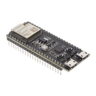
To review module reference designs please check the Documentation section on Espressif’s official website. 5.2 ESP32-S3 Development Boards For a list of the latest designs of ESP32-S3 boards please check the Development Boards section on Espressif’s official website. 5.3 Download Guidelines You can download firmware to ESP32-S3 via UART and USB. - Page 43 – USB IOs are configured to other peripherals, such as UART and LEDC. • It is recommended that the user retains control of the strapping pins to avoid the USB download function not being available in case of the above scenario. Espressif Systems Release master Submit Document Feedback...
-
Page 44: Related Documentation And Resources
Chapter 6 Related Documentation and Resources • Chip Datasheet (PDF) • Technical Reference Manual (PDF) • Chip Errata (PDF) • Chip Variants • Modules • Development Boards • Espressif KiCad Library • ESP Product Selector • Regulatory Certificates • User Forum (Hardware) •... - Page 45 Chapter 6. Related Documentation and Resources Espressif Systems Release master Submit Document Feedback...
-
Page 46: Glossary
Chapter 7 Glossary The glossary contains terms and acronyms that are used in this document. Term Description Capacitor-Inductor-Capacitor DDR SDRAM Double Data Rate Synchronous Dynamic Random-Access Memory Electrostatic Discharge Inductor-Capacitor Power Amplifier Resistor-Capacitor Real-Time Clock Zero-ohm resistor A zero-ohm resistor is a placeholder on the circuit so that another higher ohm resistor can replace it, depending on design cases. - Page 47 Chapter 7. Glossary Espressif Systems Release master Submit Document Feedback...
-
Page 48: Revision History
Chapter 8 Revision History 8.1 ESP Hardware Design Guidelines v1.0 This is the first version of the ESP Hardware Design Guidelines in HTML format. During the migration from PDF to HTML format, minor updates, improvements, and clarifications were made throughout the documentation. If you would like to check previous versions of the document, please submit documentation feedback. - Page 49 Chapter 8. Revision History Espressif Systems Release master Submit Document Feedback...
-
Page 50: Disclaimer And Copyright Notice
Chapter 9 Disclaimer and Copyright Notice Information in this document, including URL references, is subject to change without notice. All third party’s information in this document is provided as is with no warranties to its authenticity and accuracy. No warranty is provided to this document for its merchantability, non-infringement, fitness for any particular purpose, nor does any warranty otherwise arising out of any proposal, specification or sample.
Need help?
Do you have a question about the ESP32-S3 and is the answer not in the manual?
Questions and answers