Table of Contents
Advertisement
Quick Links
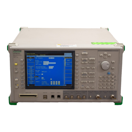
MT8820A
Radio Communication Analyzer
Manual
Service
Third Edition
To ensure that this equipment is used safely, impor-
tant safety items are explained in the MT8820A Op-
eration Manual. This document explains important
service items related to service. Read both the op-
eration manual and this document, and keep both
with the MT8820A.
Measurement Solutions
ANRITSU CORPORATION
Document No.: M-W1940BE-3.0
Advertisement
Chapters
Table of Contents
Troubleshooting

Related Manuals for Anritsu MT8820A


Summary of Contents for Anritsu MT8820A
- Page 1 Service Third Edition To ensure that this equipment is used safely, impor- tant safety items are explained in the MT8820A Op- eration Manual. This document explains important service items related to service. Read both the op- eration manual and this document, and keep both with the MT8820A.
- Page 2 BEFORE using the equipment. Some or all of the following five symbols may not be used on all Anritsu equipment. In addition, there may be other labels attached to products which are not shown in the diagrams in this manual.
-
Page 3: For Safety
Always request repair by a trained engineer who understands the haz- ards. Anritsu Corporation will not accept liability for any injuries sustained as a result of opening the equipment covers. CAUTION Before changing the fuses, ALWAYS remove the power cord from the poweroutlet and replace the blown fuses. - Page 4 Trademark MS, Microsoft, MS-DOS, Windows and Visual Basic are registered trademarks of Microsoft Corporation. IBM and AT are registered trademarks of International Business Machi- nes Corporation. iv iv iv iv...
-
Page 5: About This Manual
About This Manual The MT8820A Radio Communication Analyzer Service Manual describes how to locate a faulty module of MT8820A in trouble and repair it by mod- ule replacement. It does not mention repairing the faulty module itself. This manual is prepared for service men of Anritsu or its agencies who have completed the necessary training courses and have complete under- standing about the danger of fire or electric shock. -
Page 6: Table Of Contents
Table of Contents For Safety ........... About This Manual ........Section 1 General........Section 2 Circuit Description ....Outline................Circuit Description of Each Unit ........2-15 Section 3 Troubleshooting ....... Outline................Service Kits ..............Instruments Required for Troubleshooting ....Circuit Reference ............Overall Troubleshooting.......... -
Page 7: General
Section Section 1 1 1 1 General General General General This service manual explains how to maintain the MT8820A Radio Com- munication Analyzer. Section 1 describes the configuration of this man- ual. Section 1 General Describes the service manual configuration. - Page 8 Section 1 Section 1 General General Section 1 Section 1 General General 1- 1- 1- 1-2 2 2 2 ..
- Page 9 Section Section 2 Circuit Description Section Section 2 Circuit Description 2 Circuit Description 2 Circuit Description Outline ............... 2.1.1 Outline of Circuitry......... 2.1.2 Power Line Description ......... 2.1.3 Signal Lines Description........ 2-10 Circuit Description of Each Unit......... 2-15 2.2.1 A01 Main CPU Unit ........2-15 2.2.2 A41, A42 WCDMA COM Unit......
-
Page 10: Outline
Section 2 Circuit Description Section 2 Circuit Description 2.1 Outline This section explains the unit configuration of the MT8820A and the block diagram for each unit. 2.1.1 Outline of Circuitry Table 2-1 gives the unit outline and Figure 2-1 shows the overall block diagram. - Page 11 Outline Outline Outline Outline Table 2-1 Outline of Circuitry (Continued) A No. Name Description DAC / ADC • The DAC/ADC board provides two I/O routes for downlink and uplink signals. • Digital to analog conversion of downlink baseband signal. • Analog to digital conversion of uplink IF signal.
- Page 12 Section 2 Circuit Description Section 2 Circuit Description Section 2 Circuit Description Section 2 Circuit Description Table 2-1 Outline of Circuitry (Continued) A No. Name Description • Low-pass filter for the SPA RF input section. A7101 INPUT LPF The signal from the RF S-ATT for SPA is A7201 output to the 1st Mixer through LPF.
- Page 13 Outline Outline Outline Outline Table 2-1 Outline of Circuitry (Continued) A No. Name Description • Contains 10 MHz reference crystal oscillator. REFERENCE • Generates 100 MHz signal synchronized with the 10 MHz oscillator signal that is the reference clock, and then sends the 800 MHz signal (100 MHz multiplied by 8) to the RF and LOCAL units.
- Page 14 Section 2 Circuit Description Section 2 Circuit Description Section 2 Circuit Description Section 2 Circuit Description Table 2-1 Outline of Circuitry (Continued) A No. Name Description • Generates key-code data and interrupts PANEL depending on key entries. CONTROL • Generates rotary knob rotation count and interrupts.
- Page 15 Outline Outline Outline Outline A71 RF AD/DA control (Serial Data) Demod IF A72 RF AD/DA control (Serial Data) A41 WCDMA COM A51 WCDMA BB A02 DAC/ADC A01 Main CPU A71 RF Aux Out Digital I,Q Frame Inter Spreader WCDMA Analog I,Q coder polator 1 Controller...
- Page 16 Section 2 Circuit Description Section 2 Circuit Description Section 2 Circuit Description Section 2 Circuit Description 2- 2- 2- 2-8 8 8 8...
- Page 17 Outline Outline Outline Outline 2.1.2 Power Line Description The power supply unit provides twelve secondary power outputs: +3.3 V, +5.0 V (Digital), ±5.0 V (Analog), +5.0 V (four USBs), ±12 V, +24 V and standby +12 V (S). All power for the units and connectors are output through the A05 mother board.
-
Page 18: Signal Lines Description
Section Section Section Section 2 2 2 2 Circuit Description Circuit Description Circuit Description Circuit Description 2.1.3 Signal Lines Description Figure 2-2 shows the signal lines that go through the A05 mother board. 2- 2- 2- 2-10... - Page 19 Outline Outline Outline Outline Fig. 2-2 Signal Line Diagram PCI 1 PCI 2 PCI 3 PCI 4 PCI 5 PCI 6 PCI 7 PCI 8 PCI 9 PCI 10 PCI 11 PCI 12 PCI 13 Local1 Local2 Main TDMA Cdma2K WCDMA WCDMA Meas...
- Page 20 Section 2 Circuit Description Section 2 Circuit Description Section 2 Circuit Description Section 2 Circuit Description Fig. 2-2 Signal Line Diagram (Continued) PCI 1 PCI 2 PCI 3 PCI 4 PCI 5 PCI 6 PCI 7 PCI 8 PCI 9 PCI 10 PCI 11 PCI 12...
- Page 21 Outline Outline Outline Outline Fig. 2-2 Signal Line Diagram (Continued) PCI 1 PCI 2 PCI 3 PCI 4 PCI 5 PCI 6 PCI 7 PCI 8 PCI 9 PCI 10 PCI 11 PCI 12 PCI 13 Local1 Local2 Main TDMA Cdma2K WCDMA WCDMA...
- Page 22 Section 2 Circuit Description Section 2 Circuit Description Section 2 Circuit Description Section 2 Circuit Description 2- 2- 2- 2-14...
-
Page 23: Circuit Description Of Each Unit
Insert the A01 main CPU to the digital board shielding case from the top of the MT8820A. The A01 main CPU is a control circuit that controls the MT8820A func- tions and all units. Figure 2-3 shows the A01 main CPU unit block diagram. For signals that go through the A05 mother board, see Section 2.1.3. - Page 24 • Compact Flash Compact Flash socket provided. IDE interface connection (M1543), power: 3.3 V, capacity: 128 Mbytes Memory for storing programs that provide MT8820A functions. The memory contents can be rewritten by downloading from the PC card. • KEY/PANEL CONTROL interface...
- Page 25 Circuit Description of Each Unit Circuit Description of Each Unit Circuit Description of Each Unit Circuit Description of Each Unit Fig. 2-3 A01 Main CPU Block Diagram 2- 2- 2- 2-17...
-
Page 26: A41, A42 Wcdma Com Unit
Section 2 Circuit Description 2.2.2 A41, A42 WCDMA COM Unit Insert the A41/A42 WCDMA COM to the digital board shielding case from the top of the MT8820A. For signals that go through the A05 mother board, see Section 2.1.3. • Function overview ·... - Page 27 Circuit Description of Each Unit Circuit Description of Each Unit Circuit Description of Each Unit Circuit Description of Each Unit • Basic functions · Signaling processing for WCDMA terminal measurement/test (Functions for Layer 3, Layer 2, and Layer 1 (up to frame coding/decoding) ·...
- Page 28 Section Section 2 Circuit Description 2 Circuit Description Section Section 2 Circuit Description 2 Circuit Description 2- 2- 2- 2-20...
-
Page 29: A51, A52 Wcdma Bb Unit
Circuit Description of Each Unit 2.2.3 A51, A52 WCDMA BB Unit Insert the A51/A52 WCDMA BB to the digital board shielding case from the top of the MT8820A. For signals that go through the A05 mother board, see Section 2.1.3. • Function overview... - Page 30 Section Section 2 Circuit Description Section Section 2 Circuit Description 2 Circuit Description 2 Circuit Description 2- 2- 2- 2-22...
-
Page 31: A61, A62 Meas Dsp Unit
2.2.4 A61, A62 MEAS DSP Unit Insert the A61/A62 MEAS DSP to the digital board shielding case from the top of the MT8820A. For signals that go through the A05 mother board, see Section 2.1.3. Figure 2-6 shows the A61/A62 MEAS DSP unit block diagram and Figures 2-7 shows Interrupts Signal to DSP. - Page 32 Section Section Section Section 2 Circuit Description 2 Circuit Description 2 Circuit Description 2 Circuit Description 2- 2- 2- 2-24...
- Page 33 Circuit Description of Each Unit Circuit Description of Each Unit Circuit Description of Each Unit Circuit Description of Each Unit • Measurement For the digital sample from the DAC/ADC board, frequency conversion and filtering are performed. Then, it is stored in the waveform memory.
- Page 34 Section 2 Circuit Description Section 2 Circuit Description Section 2 Circuit Description Section 2 Circuit Description • Communication between DSPs Communication with other the MainDSP and the SubDSP are performed through the Link port. • Communication with other CPUs Communication between the CPUs are performed by using the Common RAM, RAM in Core-FPGA and communication control signals, through the C-PCI bus.
-
Page 35: A02 Dac/Adc Unit
2.2.5 A02 DAC/ADC Unit Insert the A02 DAC/ADC unit in the digital board shielding case from the top of the MT8820A. For signals that go through the A05 mother board, see Section 2.1.3. Figures 2-8 (A) and (B) show the A02 DAC/ADC unit block diagram. - Page 36 Section 2 Circuit Description Section 2 Circuit Description Section 2 Circuit Description Section 2 Circuit Description 2- 2- 2- 2-28...
- Page 37 2.2 Circuit Description of Each Circuit Description of Each Circuit Description of Each Unit Circuit Description of Each Unit Unit Unit 2- 2- 2- 2-29...
-
Page 38: A71, A72 Rf Unit
• (A7102, A7202) OUTPUT AMP • (A7103, A7203) RF • (A7104, A7204) IF Insert the A71/A72 RF unit in the shielding case from the top of the MT8820A. Figure 2-9 shows the A71/A72 RF unit block diagram. 2- 2- 2- 2-30... - Page 39 Circuit Description of Each Unit Circuit Description of Each Unit Circuit Description of Each Unit Circuit Description of Each Unit ATT Control Voltage Reader ALC OFF OutPut Level Setting ALC ON Reference Voltage A7102/7202 Carrier leak adj. OUTPUT AMP ~ HSM88 ~...
- Page 40 Section 2 Circuit Description Section 2 Circuit Description Section 2 Circuit Description Section 2 Circuit Description 2- 2- 2- 2-32...
-
Page 41: A7101, A7201 Input Lpf
Circuit Description of Each Unit Circuit Description of Each Unit Circuit Description of Each Unit Circuit Description of Each Unit 2.2.7 A7101, A7201 Input LPF The A7101/A7201 input LPF is located in the A71/A72 RF unit. Low-pass filter for the SPA RF input section. The signal from the RF S- ATT for SPA is output to the 1st Mixer through LPF. -
Page 42: A81, A82 Local Unit
2.2.11 A81, A82 Local Unit The local unit is contained in an aluminum shielding case and connected to the A05 mother board from the bottom of the MT8820A. Using the 800 MHz signal supplied from the A04 REFERENCE unit as the reference, the local unit generates signal for YTO PLL depending on the output/reception frequency for the RF unit SPA/SG section and outputs it to the RF unit. - Page 43 Circuit Description of Each Unit Circuit Description of Each Unit Circuit Description of Each Unit Circuit Description of Each Unit • SG sampling signal generator Generates sampling signal for YTO PLL for RF unit SG. relationships between SG output frequency and YTO frequency are given below.
- Page 44 Section 2 Circuit Description Section 2 Circuit Description Section 2 Circuit Description Section 2 Circuit Description • Calculating parameters IF Fyto < 5900.000 000 IF AB = odd number (45, 47, 49, etc.) M = INT{ ( AB+1 ) / 2 } SAMOSCPOL = –1 SELECT CASE CD CD=00 to 41...
- Page 45 Circuit Descript Circuit Description of Each Unit Circuit Descript Circuit Descript ion of Each Unit ion of Each Unit ion of Each Unit CD=00 to 57 YTOPLLPOL = –1 CD=58 to 99 YTOPLLPOL = +1 END SELECT Nset = INT[{(200 MHz × M) / ABS( 200 MHz × M– Fyto +YTOPLLPOL × DDScal )}+ 0.5] ENDIF FDDS = ABS( M ×...
- Page 46 Section 2 Circuit Description Section 2 Circuit Description Section 2 Circuit Description Section 2 Circuit Description Figure 2-10 shows the A81/A82 local unit block diagram. SG REF SPA REF SG Sample SPA Sample 29 M 29 M 200 MHz ±(1.07 to 5.88 MHz) 200 MHz±(1.07 to 5.88 MHz) ±2 MHz ±2 MHz...
-
Page 47: A04 Reference Unit
MHz signal (100 MHz multiplied by 8) to the RF and local units. When a 10 MHz- or 13 MHz-external reference signal is input from the MT8820A, it generates a 800 MHz signal by multiplying by 8 the 100 MHz signal synchronized with the 10 and 13 MHz signals as reference clocks. - Page 48 Section 2 Circuit Description Section 2 Circuit Description Section 2 Circuit Description Section 2 Circuit Description 2- 2- 2- 2-40...
- Page 49 Circuit Description of Each Unit Circuit Description of Each Unit Circuit Description of Each Unit Circuit Description of Each Unit S/N ratio: –165 dBc/Hz – – – – 9dBm min level 9dBm min level 9dBm min level 9dBm min level Unlock Status Ext_REF in 10 MHz/13 MHz...
- Page 50 Section 2 Circuit Description Section 2 Circuit Description Section 2 Circuit Description Section 2 Circuit Description 2- 2- 2- 2-42...
-
Page 51: A05 Mother Board
Circuit Description of Each Unit Circuit Description of Each Unit Circuit Description of Each Unit 2.2.13 A05 Mother Board The A05 mother board is on the bottom of the MT8820A. For A05 mother board internal connections, see Section 2.1.3. 2- 2- 2- 2-43... -
Page 52: A07 Panel Control Unit
Section 2 Circuit Description Section 2 Circuit Description 2.2.14 A07 Panel Control Unit The A07 panel control unit is on the front of the MT8820A, outside the shielding case. For signals that go through the A05 mother board, see Section 2.1.3. - Page 53 Circuit Description of Each Unit Circuit Description of Each Unit Circuit Description of Each Unit Circuit Description of Each Unit • Interfaces Connect the cable to the A05 mother board for communications with the A01 main CPU. Connect the cable to the front key panel. Connect the power cable to the inverter.
- Page 54 Section 2 Circuit Description Section 2 Circuit Description Section 2 Circuit Description Section 2 Circuit Description ENCODER ROTATE ENCODER PUSH +3.3V +5V(D) ENCODER +12V COUNTER NINT2 INTERRUPT Management 2 POWER OFF INTERRUPT CONTROL MASK STATUS REGISTER COL 8 NINT1 INTERRUPT KEY CODE 割込み...
-
Page 55: Power Supply Unit
The power supply unit contains the power inlet and power switch accessed from the rear panel and mounted on the rear of the MT8820A. It converts the primary power (100 to 120 VAC or 200 to 240 VAC) to nine secondary powers: +3.3 V, +5 V (D), +5 V (USB), ±5 V (A), ±12 V, +12 V (S) -
Page 56: A21, A22 Tdma Com Unit
Section 2 Circuit Description 2.2.16 A21, A22 TDMA COM Unit Insert the A21/A22 TDMA COM unit to the digital-board shielding case from the top of the MT8820A. For the signals that go through the A05 Mother board, see Section 2.1.3. • Function overview ・... - Page 57 Circu Circuit Description of Each Unit it Description of Each Unit Circu Circu it Description of Each Unit it Description of Each Unit Timing Generator FPGA1 (EP20K100EFC324) Generates the clock signal of the frequency of 16-multiples or integer- multiples of transmission speed specified by each communication system.
- Page 58 Section 2 Circuit Description Section 2 Circuit Description Section 2 Circuit Description Section 2 Circuit Description Rx Signal Processing A/D Converter AD9042AST Converts the analog IF input signal to the digital IF signal by using A/D converter. IF signal frequency: 4.8 MHz −...
- Page 59 Circuit Descri Circuit Descri Circuit Descri Circuit Description of Each Unit ption of Each Unit ption of Each Unit ption of Each Unit JTAG FPGA2 Connector Com CPU SH7729 Interpolation Serial IF 133 MHz RS232C Filter (x2) Dual Modulation Encode Connector ( I ) Port...
- Page 60 Section 2 Circuit Description Section 2 Circuit Description Section 2 Circuit Description Section 2 Circuit Description 2- 2- 2- 2-52...
-
Page 61: A03 Audio Unit
Description of Each Unit 2.2.17 A03 AUDIO Unit Insert the A03 AUDIO to the digital board shielding case from the top of the MT8820A. For signals that go through the A05 Mother board , see Section 2.1.3. • Function overview ・... - Page 62 Section 2 Circuit Description Section 2 Circuit Description Section 2 Circuit Description Section 2 Circuit Description 2- 2- 2- 2-54...
- Page 63 Circuit Description of Each Unit Circuit Description of Each Unit Circuit Description of Each Unit Circuit Description of Each Unit DSP 1 Core A FIFO S←P FIFO P→S P←S FIFO DSP 1 FIFO S→P Core B FIFO 9054 P→S P←S FPGA2 FIFO DSP 2...
- Page 64 Section 2 Circuit Description Section 2 Circuit Description Section 2 Circuit Description Section 2 Circuit Description 2- 2- 2- 2-56 56..
- Page 65 Section 3 3 3 3 Troubleshooting Section Troubleshooting Section Section Troubleshooting Troubleshooting Outline ............... Service Kits..............Instruments Required for Troubleshooting ....Circuit Reference ............Overall Troubleshooting ..........3.5.1 Outline of Troubleshooting Procedure ..3.5.2 Power and Control Troubleshooting....3.5.3 Output Frequency Troubleshooting....3-10 3.5.4 Input Frequency Troubleshooting ....
-
Page 66: Troubleshooting
Troubleshooting Troubleshooting 3.1 Outline This section describes how to detect a fault when an error occurs in the MT8820A. 3.2 Service Kits The service kit ordering number is 34Y130332. Table 3-1 shows the con- tents of the kit. Table 3-1 Service Kits Accessory No. - Page 67 Service Kits Service Kits Service Kits Service Kits Table 3-1 Service Kits (Continued) Accessory No. Drawing No. Q'ty Remarks Name 34Y127777 EXTENDER-LO CABLE (X11) X13 ( for LOCAL UNIT) 332U45588a (X1) 34J127172G BNC-MMCX CABLE 0.8DS-PBE BNC-PJ-0.8D MMCX-LP-0.8D 34J122139T MMCX-P-LP-CABLE 0.8DS-PBE MMCX-SP-0.8D MMCX-LP-0.8P NO.1305...
- Page 68 Section Section Section Section 3 3 3 3 Troubleshooting Troubleshooting Troubleshooting Troubleshooting Table 3-1 Service Kits (Continued) Accessory No. Drawing No. Q'ty Remarks Name S4J10001F Extender Cable 1000 RG-55A/U BNC-P BNC-P S4W10184C Extender Cable Special 3D-2V SMA-P SMA-P 10 S4J10319 NP-SMAJ (SMA-AD12-SF(12)) Adaptor...
-
Page 69: Instruments Required For Troubleshooting
Instruments Required for Troubleshooting 3.3 Instruments Required for Troubleshooting Table 3-2 lists the instruments necessary for troubleshooting. Table 3-2 Instruments Required for Troubleshooting Instrument Major Performance (Anritsu) Frequency Counter 30 MHz to 2.7 GHz (MF2412B) Spectrum Analyzer 30 MHz to 2.7 GHz... -
Page 70: Circuit Reference
Troubleshooting Troubleshooting 3.4 Circuit Reference The units and printed circuit (PC) boards for the MT8820A have module names beginning with “MM.” (For purchased components that are defined as exchangeable modules, product names assigned by manufactures are used as module model names.) -
Page 71: Overall Troubleshooting
Overall Troubleshooting Overall Troubleshooting Overall Troubleshooting Overall Troubleshooting 3.5 Overall Troubleshooting 3.5.1 Outline of Troubleshooting Procedure Figure 3-1 shows the outline for the troubleshooting procedure. Start Locate a faulty unit related to power or control (Section 3.5.2) Locate a faulty unit related to output frequency (Section 3.5.3) Locate a faulty unit related to reception frequency (Section 3.5.4) -
Page 72: Power And Control Troubleshooting
Section Section Section Section 3 3 3 3 Troubleshooting Troubleshooting Troubleshooting Troubleshooting 3.5.2 Power and Control Troubleshooting Figure 3-2 shows the flowchart for locating a faulty block related to power or control. Start [Location to be checked] “Stby” LED goes ON in “Stby”... - Page 73 Overall Troubleshooting Overall Troubleshooting Overall Troubleshooting Overall Troubleshooting From previous page Three fans running? Three fans all stopped? Stopped fan is faulty. Power supply unit or all fans are faulty. Key entries available? All key entries unavail- A01, A07, or key pan- able? el is faulty.
-
Page 74: Output Frequency Troubleshooting
Section Section Section Section 3 3 3 3 Troubleshooting Troubleshooting Troubleshooting Troubleshooting 3.5.3 Output Frequency Troubleshooting Figure 3-3 shows the flowchart to locate a faulty block related to output frequency settings. Start With CW, –10 dBm, and MAIN output ON, observe the output signal with a spectrum analyzer while changing the frequency from 30 MHz to 2.7 GHz. - Page 75 Overall Troubleshooting Overall Troubleshooting Overall Troubleshooting Overall Troubleshooting Table 3-4 Signal Check Point for A04 REFERENCE UNIT Part No. Name Frequency Level X3 to X6 800 MHz OUTPUT 800 MHz 0 dBm ±3 dB 10 MHz OUTPUT 10 MHz TTL Level Checking the above points requires the cable noted below.
- Page 76 Section Section Section Section 3 3 3 3 Troubleshooting Troubleshooting Troubleshooting Troubleshooting Table 3-6 Signal Check Point for A71, A72 RF UNIT Part No. Name Frequency Level SPA YTO Carrier+ –6 dBm ±2 dB MONITOR 4.1825 (A7103/7203 RF) 2nd LO MONITOR 4 GHz –17 dBm ±2 dB (A7103/7203 RF)
-
Page 77: Input Frequency Troubleshooting
Overall Troubleshooting Overall Troubleshooting Overall Troubleshooting Overall Troubleshooting 3.5.4 Input Frequency Troubleshooting Figure 3-5 shows the flowchart to locate a faulty block related to reception frequency settings. Start Synchronize external SG with 10 MHz Ref signal, input CW, –5 dBm from external SG and set main unit input level –5 dBm. -
Page 78: Output Level Troubleshooting
Section Section Section Section 3 3 3 3 Troubleshooting Troubleshooting Troubleshooting Troubleshooting 3.5.5 Output Level Troubleshooting Figure 3-6 shows the flowchart to locate a faulty block related to level set- tings. Start With CW, –10 dBm, observe the output level with power meter while changing the frequency from the lower to the upper limit. - Page 79 Overall Troubleshooting Overall Troubleshooting Overall Troubleshooting Overall Troubleshooting [Location to be checked] In settings where correct level is not output, discon- nect W3, terminate DI- VIDER X3 with 50 Ω and re-execute full calibration. With X3 terminated with AUX output level is Disconnect A71 RF 50 Ω, output level is cor- correct?
-
Page 80: Txpower Troubleshooting
Section Section Section Section 3 3 3 3 Troubleshooting Troubleshooting Troubleshooting Troubleshooting 3.5.6 TxPower Troubleshooting Figure 3-7 shows the flowchart to locate a faulty block related to TxPower. Start Perform full calibration on the main unit and input un- modulated signal with 1 GHz frequency, calibrated to level –5 dBm ±0.1 dB to the MAIN terminal. - Page 81 Overall Troubleshooting Overall Troubleshooting Overall Troubleshooting Overall Troubleshooting [Location to be checked] Disconnect W4, terminate DIVIDER X2 with 50 Ω, and re-execute full calibra- tion. With X2 terminated with Disconnect W3 and DIVIDER is faulty. 50 Ω, correct level is measure DIVIDER X3 measured? with Power Meter.
- Page 82 Section Section Section Section 3 3 3 3 Troubleshooting Troubleshooting Troubleshooting Troubleshooting 3- 3- 3- 3-18 18..
- Page 83 Section Section 4 4 4 4 Adjustment and Section Section Adjustment and Adjustment and Adjustment and C C C C ompensation ompensation ompensation ompensation Outline ............... Instruments Required for Adjustment and Compensation............. Change Parts on A01 MAIN CPU UNIT ....Carrier Leak Adjustment..........
-
Page 84: Adjustment And Compensation
Section 4 Section 4 Adjustment and Adjustment and C C C C ompensation ompensation Section 4 Section 4 Adjustment and Adjustment and ompensation ompensation 4.1 Outline This section describes the adjustment and compensation procedures ne- cessary after module replacement. Table 4-1 lists adjustment and compensation necessary for the repaired or replaced unit. -
Page 85: Instruments Required For Adjustment And Compensation
Tables 4-2 and 4-3 list the instruments required for adjustment and com- pensation. Table 4-2 Instruments Required for Adjustment Instrument Model Name Manufacture Major Performance Spectrum Analyzer MS2665C Anritsu 30 MHz to 2.7 GHz Table 4-3 Instruments Required for Compensation Instrument Model Name Manufacture Major Performance Power Meter ML2437A Anritsu 30 MHz to 2.7 GHz... -
Page 86: Change Parts On A01 Main Cpu Unit
Section 4 Section 4 Adjustment and Adjustment and C C C C ompensation ompensation Section 4 Section 4 Adjustment and Adjustment and ompensation ompensation 4.3 Change Parts on A01 MAIN CPU UNIT After replacing the A01 main CPU unit, remove the compact flash card and ROM from the old unit and mount them to the new unit. -
Page 87: Carrier Leak Adjustment
Leak Adjustment 4.4 Carrier Leak Adjustment After replacing the A02 DAC/ADC unit or the A71/A72 RF unit, adjust the A02 DAC/ADC unit while it is mounted on MT8820A. Carrier leakage must be adjusted. (1) Setup Connect the MT8820A MAIN1 Output connector to the spectrum analyzer RF Input connector using a coaxial cable. - Page 88 Set the MT8820 output to “Vector modulation” by GPIB control. (Com- mand: “MHCWOUT 3”) Set the MT8820A output level to –14.9 dBm. (Set test conditions to make the I/Q level the lowest.) On MT8820A, set any carrier frequency in the output frequency range.
- Page 89 Carrier Leak Adjustment Carrier Leak Adjustment Carrier Leak Adjustment Carrier Leak Adjustment (3) Carrier Leak Adjustment Fig. 4-3 Carrier Leak Adjustment A02 DAC/ADC A02 DAC/ADC A02 DAC/ADC A02 DAC/ADC Fig. 4-4 Carrier Leak Level Adjustment ( A02 DAC/ADC ) 4- 4- 4- 4-7 7 7 7...
-
Page 90: Output Level And Input Frequency Character Compensation
4.5 Output Level and Input Frequency Character Compensation After replacing the following listed MT8820A units, re-compensate the output level and input frequency character. • A02 DAC/ADC UNIT • A71/A72 RF UNIT • HPS-2H(5), (POWER DIVIDER) • S-ATT 4S/1SW •... -
Page 91: Fm Deviation Adjustment
FM Deviation Adjustment FM Deviation Adjustment FM Deviation Adjustment FM Deviation Adjustment 4.6 FM Deviation Adjustment After replacing the following listed MT8820A units, re-adjust the FM de- viation character. • A03 AUDIO unit • A21/A22 TDMA COM unit • A81/A82 LOCAL unit... - Page 92 Condition: Modulation Analyzer LPF 15 kHz Note: Before performing other adjustments or performance test after abo- ve FM deviation adjustment, turn Off and then On the MT8820A power switch to return the internal settings to the normal condition. 4- 4- 4- 4-10...
- Page 93 Section 5 5 5 5 Mechanical Configuration Section Mechanical Configuration Section Section Mechanical Configuration Mechanical Configuration Outline ............... Cabinet and Shield Case Assembly ......Main Unit Removal ............ 5.3.1 Removing A01 MAIN CPU (1)....... 5.3.2 Removing A41, A42 WCDMA COM (4, 10) .. 5.3.3 Removing A51, A52 WCDMA BB (5, 9) ..
-
Page 94: Mechanical Configuration
Mechanical Configuration Mechanical Configuration 5.1 Outline This section explains how to remove MT8820A components for repair. The numbers pointing to units or components in Figures 5-1 to 5-4 corre- spond to those in the parts lists for Tables 5-1 to 5-3. -
Page 95: Cabinet And Shield Case Assembly
Cabinet and Shield Case Assembly Cabinet and Shield Case Assembly Cabinet and Shield Case Assembly Cabinet and Shield Case Assembly 5.2 Cabinet and Shield Case Assembly (1) Removing top cover (38) Step Procedure Remove four feet (32), (33), (36) and (37) from the top. (Figure 5-3) From the rear, remove the screw fixing the top cover (38). - Page 96 Section Section Section Section 5 5 5 5 Mechanical Configuration Mechanical Configuration Mechanical Configuration Mechanical Configuration (5) Removing Rear Panel (53) Step Procedure Remove four legs (34), (35), (36) and (37) on the rear. (Figure 5-3) Remove side handle (41) and side cover (40). (Figure 5-3) Remove rear cover (54).
-
Page 97: Main Unit Removal
Main Unit Removal Main Unit Removal Main Unit Removal Main Unit Removal 5.3 Main Unit Removal 5.3.1 Removing A01 MAIN CPU (1) Step Procedure Remove the shield cover. (See (2) in Section 5.2.) Remove cable W31 from LCD (45). Raise the ejector for the A01 MAIN CPU (1) and pull out the unit. (Figure 5-1) 5.3.2 Removing A41, A42 WCDMA COM (4, 10) Step... -
Page 98: Removing A71, A72 Rf (14, 15)
Section Section Section Section 5 5 5 5 Mechanical Configuration Mechanical Configuration Mechanical Configuration Mechanical Configuration 5.3.6 Removing A71, A72 RF (14, 15) Step Procedure CAUTION : Turning the case upside down with the shield cover (51) removed may cause the A71/A72 RF unit to fall out. Remove the top (38) and bottom covers (39). -
Page 99: Removing A05 Mother Board (19)
Remove mother panel (47) from the power divider. (Figure 5-2) Remove all cables from A05 mother board. Remove screws fixing A05 mother board. (Figure 5-2) Pull out A05 mother board from bottom of MT8820A. (Figure 5-2) 5.3.10 Removing A07 PANEL CONTROL (20) Step Procedure Remove front panel (50). -
Page 100: Removing S-Att (23) And (24)
Section Section Section Section 5 5 5 5 Mechanical Configuration Mechanical Configuration Mechanical Configuration Mechanical Configuration 5.3.14 Removing S-ATT (23) and (24) Step Procedure Remove RF unit (14, 15). (See Section 5.3.6.) S-ATT 4S/1SW (23) and S-ATT 6S/2SW (24) are mounted on the RF unit. -
Page 101: Built-In Option Unit
Built-in Option Unit Built-in Option Unit Built-in Option Unit Built-in Option Unit 5.4 Built-in Option Unit Note: When installing options in the digital board shielding case, assign C-PCI slot numbers sequentially from 1 (the slot where the A01 main CPU board is inserted) to 13 toward the rear side. 5.4.1 Built-in Option Digital Board UNIT Step Procedure... -
Page 102: Built-In Option Analog Unit (For Parallel Phone)
Section Section Section Section 5 5 5 5 Mechanical Configuration Mechanical Configuration Mechanical Configuration Mechanical Configuration 5.4.2 Built-in Option Analog Unit (for Parallel Phone) Step Procedure Remove top cover (38). (See (1) in Section 5.2.) Insert A72 RF2 (15). (Figure 5-1) Remove bottom cover (39). -
Page 103: Parts Lists
Parts Lists Parts Lists Parts Lists Parts Lists 5.5 Parts Lists Table 5-1 Module List Order No. Model No. A No. Name Q’ty 34Y126600 MM800057 MAIN CPU 34Y126602 MM800064 TDMA COM 34Y126604 MM800065 CDMA2K COM 34Y126606 MM800066 WCDMA COM 34Y126608 MM800067 WCDMA BB 34Y126610... - Page 104 Section Section Section Section 5 5 5 5 Mechanical Configuration Mechanical Configuration Mechanical Configuration Mechanical Configuration Table 5-2 Mechanical and Other Parts List Parts No. Name Remarks Q’ty 32E11801A Foot, Front Right Side Bottom 32E11801B Foot, Front Left Side Bottom 32E11802A Foot, Front Left Side Top 32E11802B Foot, Front Right Side Top 32E11803A Foot, Rear Right Side Bottom...
- Page 105 Parts Lists Parts Lists Parts Lists Parts Lists 10 11 Fig. 5-1 5- 5- 5- 5-13...
- Page 106 Section Section 5 5 5 5 Mechanical Configuration Section Section Mechanical Configuration Mechanical Configuration Mechanical Configuration Fig. 5-2 5- 5- 5- 5-14...
- Page 107 Parts Lists Parts Lists Parts Lists Parts Lists Fig. 5-3 5- 5- 5- 5-15...
- Page 108 Section Section 5 5 5 5 Mechanical Configuration Section Section Mechanical Configuration Mechanical Configuration Mechanical Configuration Fig. 5-4 5- 5- 5- 5-16 16..
Need help?
Do you have a question about the MT8820A and is the answer not in the manual?
Questions and answers