Table of Contents
Advertisement
Quick Links
Advertisement
Table of Contents

Related Manuals for MSI MS-98N1


Summary of Contents for MSI MS-98N1
- Page 1 MS-98N1 Industrial Computer Board User Guide...
-
Page 2: Table Of Contents
Contents Regulatory Notices ....................... 4 Safety Information ......................7 Specifications ....................... 8 Motherboard Overview ....................11 Rear I/O Panel ......................12 Power Jack ......................12 DisplayPort ......................12 Connector ..................12 VGA Port ......................... 12 RJ-45 LAN Jack ..................... 13 USB 3.2 Gen 1 Port .................... - Page 3 JPWR1: DC-In Power Connector (Optional) ..................23 JSATA_PWR1: SATA Power Connector .................... 23 Graphics Connectors ..................... 24 JINV1: LVDS Inverter Box Header ....................24 JLVDS1: LVDS+eDP Wafer Connector ....................25 Other Connectors ....................28 SYSFAN1: System Fan Box Header ....................28 JKBMS1: PS/2®...
-
Page 4: Regulatory Notices
Regulatory Notices FCC-B Radio Frequency Interference Statement This equipment has been tested and found to comply with the limits for a Class B digital device, pursuant to part 15 of the FCC rules. These limits are designed to provide reasonable protection against harmful interference in a residential installation. - Page 5 ∙ Users should contact the local authorized point of collection for recycling and disposing of their end-of-life products. ∙ Visit the MSI website and locate a nearby distributor for further recycling information. ∙ Users may also reach us at gpcontdev@msi.com for information regarding proper Disposal, Take-back, Recycling, and Disassembly of MSI products.
- Page 6 ∙ Reduced solid waste production through take-back policy Copyright and Trademarks Notice Copyright © Micro-Star Int’l Co., Ltd. All rights reserved. The MSI logo used is a registered trademark of Micro-Star Int’l Co., Ltd. All other marks and names mentioned may be trademarks of their respective owners. No warranty as to accuracy or completeness is expressed or implied.
-
Page 7: Safety Information
Safety Information ∙ The components included in this package are prone to damage from electrostatic discharge (ESD). Please adhere to the following instructions to ensure successful computer assembly. ∙ Ensure that all components are securely connected. Loose connections may cause the computer to not recognize a component or fail to start. -
Page 8: Specifications
Specifications Model MS-98N1 Form factor Mini-ITX Dimensions 170 x 170mm (6.7 x 6.7 inches) ∙ PC Client SKUs - Intel® Elkhart Lake J6412/ N6210 SoC 4.5W up to 12W (Burst) Processor ∙ Embedded SKUs - Intel® Atom® x6211E Processor 4.5W up to 12W (Burst) - Page 9 Model MS-98N1 ∙ Realtek® ALC897 High Definition Audio Codec - Co-lay ALC888S-VD2 Audio ∙ 3 x Connectors for audio - 1 x Line-out Jack (Rear I/O) - 2 x 5-pin headers for front audio (Headphone & Mic-in) ∙ 1 x VGA port ∙...
- Page 10 Model MS-98N1 ∙ Operating Temperature - PC Client SKUs: 0 ~ 60°C with 0.7m/s air flow Environment - Embedded SKUs: -20 ~ 70°C with 0.7m/s air flow ∙ Storage Temperature: -20 ~ 80°C ∙ Humidity: 10 ~ 90%, non-condensing Specifications...
-
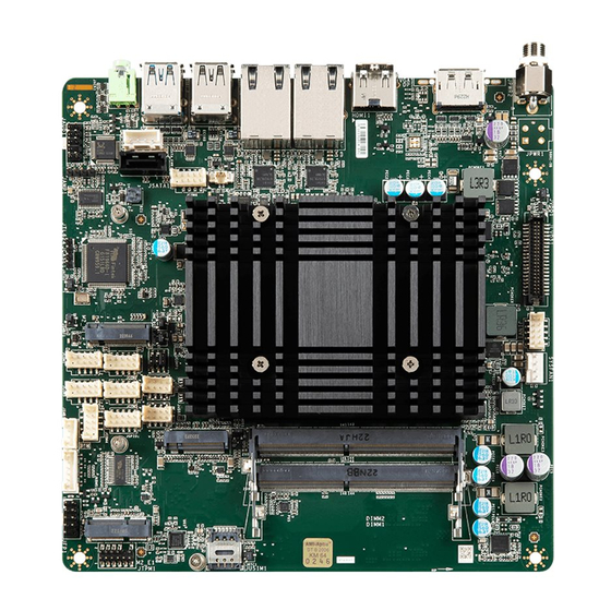
Page 11: Motherboard Overview
Motherboard Overview VGA + HDMI SKU Rear I/O Panel DP + HDMI SKU JSATA_PWR1 JPWR1 (Optional) JAUD1 JBAT1 JAMP1 JSATA1 JVDD1 JCOM6 JME_DIS1 JCOMP2 JLVDS1 JCOMP1 JCASE1 JATX1 JSMBP1 JINV1 M2_M1 SYSFAN1 JSBM1 JKBMS1 JFP1 JUSIM1 JCOMS1 M2_E1 M2_B1 DIMM1 JTPM1 JRTC1 DIMM2... -
Page 12: Rear I/O Panel
Rear I/O Panel DP + HDMI SKU USB 2.0 Port Line-Out RJ-45 Power DisplayPort Jack 3.2 Gen 1 Ports LAN Jacks Jack VGA Port USB 2.0 Port VGA + HDMI SKU Power Jack Power supplied through this jack supplies power to your system. DisplayPort DisplayPort is a digital display interface standard. -
Page 13: Rj-45 Lan Jack
RJ-45 LAN Jack The standard single RJ45 LAN jack is provided for connection to the Local Area Network (LAN). You can connect a network cable to it. Link/ Activity LED Speed LED Status Description Status Description No link 10/100 Mbps Linked Yellow 1000 Mbps... -
Page 14: Me Overview
ME Overview Board Dimension DP + HDMI SKU Unit of measurement: mm 18,50 18,05 18,95 29,18 25,32 1,15 14,45 17,00 157,48 170,00 ME Overview... -
Page 15: Vga + Hdmi Sku
VGA + HDMI SKU Unit of measurement: mm 14,45 17,00 18,50 18,05 18,95 29,43 25,07 1,15 157,48 170,00 ME Overview... -
Page 16: Suggested Chassis I/O Gap Dimension
Suggested Chassis I/O Gap Dimension Chassis Gap: 1.5mm (min) ME Overview... - Page 17 Component Contents Component Page Memory DIMM1~2: DDR4 SO DIMM Slots Storage JSATA1: SATA 3.0 6Gb/s Port M2_M1: M.2 Slot (M Key, 2242) Installing M.2 SSD Expansion Slots JUSIM1: Nano SIM Holder M2_E1: M.2 Slot (E Key, 2230) M2_B1: M.2 Slot (B Key, 2242/ 3042) Connectors Power Connectors JPWR1: DC-In Power Connector (Optional)
-
Page 18: Memory
Memory DIMM1~2: DDR4 SO DIMM Slots The SO-DIMM slots is intended for memory modules. DIMM2 DIMM1 Installing SO DIMM Slot 1. Locate the SO-DIMM slot. Align the notch on the DIMM with the key on the slot and insert the DIMM into the slot. 2. -
Page 19: Storage
Storage JSATA1: SATA 3.0 6Gb/s Port This connector is SATA 6Gb/s interface port, it can connect to one SATA device. JSATA1 JSATA1 ⚠ Important This SATA port supports hot plug. ∙ Please do not fold the SATA cable at a 90-degree angle. Data loss may result during ∙... -
Page 20: M2_M1: M.2 Slot (M Key, 2242)
M2_M1: M.2 Slot (M Key, 2242) Please install the M.2 solid-state drive (SSD) into the M.2 slot as shown below. ⚽ Video Demonstration Watch the video to learn how to Install M.2 SSD. M2_M1 Installing M.2 SSD 1. Insert your M.2 SSD into the M.2 slot at a 30-degree angle. -
Page 21: Expansion Slots
Expansion Slots M2_B1 M2_E1 JUSIM1 JUSIM1: Nano SIM Holder This holder is provided for 3G, 4G, LTE, 5G Nano SIM cards. Expansion Slots... -
Page 22: M2_E1: M.2 Slot (E Key, 2230)
M2_E1: M.2 Slot (E Key, 2230) Please install the Wi-Fi/ Bluetooch card into the M.2 slot as shown below. Feature ∙ M2_E1 slot supports PCIe x 1 & USB 2.0 signal. M2_B1: M.2 Slot (B Key, 2242/ 3042) Please install the WWAN Card/ solid-state drive (SSD) into the M.2 slot as shown below. -
Page 23: Connectors
Connectors Power Connectors JSATA_PWR1 JPWR1 JPWR1: DC-In Power Connector (Optional) This connector allows you to connect a power supply. JPWR1 DC_IN DC_IN JSATA_PWR1: SATA Power Connector This connector is used to provide power to SATA devices. JSATA_PWR1 ⚠ Important Make sure that all the power cables are securely connected to a proper power supply to ensure stable operation of the system. -
Page 24: Graphics Connectors
Graphics Connectors JINV1: LVDS Inverter Box Header The connector is provided for LCD backlight options. VCC5 VCC5 JINV1 +12V +12V INV_ON#1 L_BKLT_CTRL#1 JINV1 Connectors... -
Page 25: Jlvds1: Lvds+Edp Wafer Connector
JLVDS1: LVDS+eDP Wafer Connector This connector is designed for use with LVDS/eDP interface flat panels. When connecting your flat panel to this connector, be sure to check the panel data sheet to ensure that you set the JVDD1 LVDS power jumper to the appropriate power voltage. JLVDS1 ⚠... - Page 26 JLVDS1 eDP Panel (P1) 98N1 Motherboard (P2) eDP Panel (P1) Lane3_P EDP_LINE3_DP EDP_LINE2_DP Lane2_P Lane3_N EDP_LINE3_DN EDP_LINE2_DN Lane2_N DDC0_CLK_7513_R DDC0_DATA_7513_R LCD_VCC LCD_VDD LCD_VDD LCD_VCC LCD_VCC LCD_VDD VCC3 BKLT_EN LVDS_DETECT# LCD_GND Lane1_P LVDSA_DATA1+ EHPDET/ LVDSA_DATA0+ Lane1_N LVDSA_DATA1- LVDSA_DATA0- H_GND H_GND LVDSA_DATA3+ LVDSA_DATA2+ Lane0_P LVDSA_DATA3-...
- Page 27 JLVDS1 LVDS Panel (P1) 98N1 Motherboard (P2) LVDS Panel (P1) EDP_LINE3_DP EDP_LINE2_DP EDP_LINE3_DN EDP_LINE2_DN DDC0_CLK_7513_R DDC0_DATA_7513_R LCD_VDD LCD_VDD LCD_VDD VCC3 BKLT_EN LVDS_DETECT# RXO1+ LVDSA_DATA1+ EHPDET/ LVDSA_DATA0+ RXO0+ RXO1- LVDSA_DATA1- LVDSA_DATA0- RXO0- RXO3+ LVDSA_DATA3+ LVDSA_DATA2+ RXO2+ RXO3- LVDSA_DATA3- LVDSA_DATA2- RXO2- RXE1+ LVDSB_DATA1+ LVDSB_DATA0+ RXE0+...
-
Page 28: Other Connectors
Other Connectors SYSFAN1: System Fan Box Header The fan power connector supports system cooling fans with +12V. When connecting the wire to the connectors, always note that the red wire is the positive and should be connected to the +12V; the black wire is Ground and should be connected to GND. If the motherboard has a System Hardware Monitor chipset onboard, you must use a specially designed fan with speed sensor to take advantage of the fan control. -
Page 29: Jfp1: Front Panel Connector
JFP1: Front Panel Connector This front-panel connector is provided for electrical connection to the front panel switches & LEDs and is compliant with Intel Front Panel I/O Connectivity Design Guide. HDD LED+ POWER LED HDD LED- POWER LED JFP1 RESET SWITCH- POWER SWITCH+ RESET SWITCH+ POWER SWITCH-... -
Page 30: Jaud1: Front Audio Header
JAUD1: Front Audio Header This connector allows you to connect front panel audio. MIC_IN_L AGND MIC_IN_R JAUD1 LINE_IN_R SEN_MC SENSE_B No pin LINE_IN_L SEN_LIN JAMP1: Audio Amplifier Header The connector is used to connect audio amplifiers to enhance audio performance. AMP_RN AMP_RP JAMP1... -
Page 31: Jcom1~6: Com Port Box Headers
JCOM1~6: COM Port Box Headers These connectors are a 16550A high speed communications port that sends/ receives 16 bytes FIFOs. You can attach a serial device to it. NDCD NSIN NSOUT NDTR JCOM1~6 NDSR NRTS NCTS N/A (VCC, COM1~2) No pin JCOM6 JCOM1 JCOM2... - Page 32 JCOM1 Connector Supports RS-232/ 422/ 485, With RI/ 0V/ 5V/ 12V. JCOM2 Connector Supports RS-232/ 422/ 485, With 0V/ 5V/ 12V. JCOM3~6 Connectors Support RS-232. RS232 SIGNAL DESCRIPTION NDCD Data Carrier Detect NSIN Signal In NSOUT Signal Out NDTR Data Terminal Ready Signal Ground NDSR Data Set Ready...
-
Page 33: Jusb1~2: Usb 2.0 Box Headers
JUSB1~2: USB 2.0 Box Headers These connectors are ideal for connecting USB devices such as keyboard, mouse, or other USB-compatible devices. POWER USB- USB+ JUSB1~2 USB+ USB- POWER ⚠ Important Note that the POWER and GND pins must be connected correctly to avoid possible damage. -
Page 34: Jbat1: Cmos Battery Header
JBAT1: CMOS Battery Header If the CMOS battery is out of charge, the time in the BIOS will be reset and the data of system configuration will be lost. In this case, you need to replace the CMOS battery. JBAT1 Replacing CMOS battery 1. -
Page 35: Jumpers
Jumpers ⚠ Important Avoid adjusting jumpers when the system is on; it will damage the motherboard. JCASE1 JVDD1 JATX1 JME_DIS1 JCOMP2 JCOMP1 JSMBP1 JCMOS1 JRTC1 Jumper Name Default Setting Description COM Power Jumper 1-2: 5V (Default) JCOMP1 3-4: 12V 5-6: NRI COM Power Jumper JCOMP2 1-2: 5V... - Page 36 Jumper Name Default Setting Description SMBus Power Jumper (for JSMB1) JSMBP1 1-2: 5V (Default) 2-3: 3.3V Clear RTC Battery Jumper JRTC1 1-2: Normal (Default) 2-3: Clear RTC LVDS Power Jumper JVDD1 1-2: 3V (Default) 2-3: 5V Chassis Intrusion Jumper This connector connects to the chassis intrusion switch cable.
-
Page 37: Bios Setup
BIOS Setup This chapter provides information on the BIOS Setup program and allows users to configure the system for optimal use. Users may need to run the Setup program when: ∙ An error message appears on the screen at system startup and requests users to run SETUP. - Page 38 Control Keys ← → Select Screen ↑ ↓ Select Item Enter Select Change Value Exit General Help Previous Values Optimized Defaults Save & Reset* Screenshot capture Scroll help area upwards <K> <M> Scroll help area downwards * When you press <F10>, a confirmation window appears and it provides the modification information.
- Page 39 BIOS Item Contents Item Page The Menu Bar Main System Date System Time SATA Mode Selection Advanced Full Screen Logo Display Bootup NumLock State CPU Configuration ■ Intel Virtualization Technology ■ Active Performance-cores ■ Intel® SpeedStep(tm) ■ Intel® Speed Shift Technology ■...
- Page 40 Item Page ■ PTT Configuration ■ ME Debug Configuration ■ Anti-Rollback SVN Configuration Trusted Computing ■ Security Device Support ■ SHA256/ SHA384 PCR Bank ■ Pending Operation ■ Platform Hierarchy, Storage Hierarchy, Endorsement Hierarchy ■ Physical Presence Spec Version ■ TPM 2.0 Interface Type ■...
-
Page 41: The Menu Bar
The Menu Bar ▶ Main Use this menu for basic system configurations, such as time, date, etc. ▶ Advanced Use this menu to set up the items of special enhanced features. ▶ Boot Use this menu to specify the priority of boot devices. ▶... -
Page 42: Main
Main HDD Information ∙ RAID (VMD) Disabled: Display HDD information as plugging in status. ∙ RAID (VMD) Enabled: Display "Empty" only. *SATA_1 is for SATA port. ▶ System Date This setting allows you to set the system date. Use <Tab> key to switch between date elements. -
Page 43: Advanced
Advanced ▶ Full Screen Logo Display This BIOS feature determines if the BIOS should hide the normal POST messages with the motherboard or system manufacturer’s full-screen logo. [Enabled] BIOS will display the full-screen logo during the boot-up sequence, hiding normal POST messages. [Disabled] BIOS will display the normal POST messages, instead of the full- screen logo. - Page 44 ▶ CPU Configuration ▶ Intel Virtualization Technology Enables or disables Intel Virtualization technology. [Enabled] Enables Intel Virtualization technology and allows a platform to run multiple operating systems in independent partitions. The system can function as multiple systems virtually. [Disabled] Disables this function. ▶...
- Page 45 ▶ Intel® Speed Shift Technology Intel® Speed Shift Technology is a feature designed to enhance the performance and power efficiency of Intel processors. [Enabled] Allows the processor to manage power consumption by utilizing hardware performance state (P-State) transitions. It dynamically adjust its frequency and voltage in real-time without relying on the operating system(OS).
- Page 46 ▶ Super IO Configuration ▶ Serial Port 1/ 2/ 3/ 4/ 5/ 6 This setting enables or disables the specified serial port. » Change Settings This setting is used to change the address & IRQ settings of the specified serial port.
- Page 47 ▶ H/W Monitor (PC Health Status) These items display the current status of all monitored hardware devices/ components such as voltages, temperatures and all fans’ speeds. ▶ Smart Fan Configuration ▶ SYSFAN1 This setting enables or disables the Smart Fan function. By using Smart Fan, you can automatically adjust the fan speed of your system based on the temperature of your CPU/system, preventing overheating from causing damage to your system.
- Page 48 ▶ PCI/PCIE Device Configuration ▶ Audio Controller This setting enables or disables the detection of the onboard audio controller. ▶ Network Stack Configuration This menu provides Network Stack settings for users to enable network boot (PXE) from BIOS. ▶ Network Stack This menu provides Network Stack settings for users to enable network boot (PXE) from BIOS.
- Page 49 ▶ GPIO Group Configuration ▶ GPO0 ~ GPO3 These settings control the operation mode of the specified GPIO. ▶ PCIE ASPM settings This menu provide settings for PCIe ASPM (Active State Power Management) level for different installed devices. ▶ M2_B1/ M2_E1 Sets PCI Express ASPM (Active State Power Management) state for power saving.
-
Page 50: Boot
Boot ▶ Boot Option #1 This setting allows users to set the sequence of boot devices where BIOS attempts to load the disk operating system. Boot... -
Page 51: Security
Security ▶ Administrator Password Administrator Password controls access to the BIOS Setup utility. ▶ User Password User Password controls access to the system at boot and to the BIOS Setup utility. ▶ Chassis Intrusion Enables or disables recording messages while the chassis is opened. This function is ready for the chassis equips a chassis intrusion jumper(switch). - Page 52 ▶ PCH-FW Configuration This menu allows you to configure settings related to the PCH firmware. Firmware Information These settings show the ME Firmware Version System Integrity Value firmware information of ME Firmware Mode ME Firmware Status 1-2 the Intel ME (Management Engine).
- Page 53 ▶ Firmware Update Configuration » ME FW Image Re-Flash Enables or disables the ME Firmware Image Re-flashing. » Local FW Update Enables or disables the capability to perform a firmware update of the ME locally. ▶ PTT Configuration Intel® Platform Trust Technology (PTT) is a platform functionality for credential storage and key management used by Microsoft Windows.
- Page 54 » ME DID Message Enables or disables the display of a message containing the ME Device ID (DID). » HECI Message Check Disable This setting disables message check for BIOS boot path when sending messages. » MBP HOB Skip Setting this option will skip ME’s Memory-Based Protection (MBP) H0B region. »...
- Page 55 ▶ Trusted Computing ▶ Security Device Support This item enables or disables BIOS support for security device. When set to [Disable], the OS will not show security device. ▶ SHA256/ SHA384 PCR Bank These settings enables or disables the SHA256 PCR Bank and SHA384 PCR Bank. ▶...
- Page 56 ▶ Serial Port Console Redirection ▶ Console Redirection Console Redirection operates in host systems that do not have a monitor and keyboard attached. This setting enables or disables the operation of console redirection. When set to [Enabled], BIOS redirects and sends all contents that should be displayed on the screen to the serial COM port for display on the terminal screen.
- Page 57 ▶ Console Redirection Settings (COM1) » Terminal Type To operate the system’s console redirection, you need a terminal supporting ANSI terminal protocol and a RS-232 null modem cable connected between the host system and terminal(s). You can select emulation for the terminal from this setting. [ANSI] Extended ASCII character set.
- Page 58 ▶ Secure Boot ▶ Secure Boot Secure Boot function can be enabled only when the Platform Key (PK) is enrolled and running accordingly. ▶ Secure Boot Mode Selects the secure boot mode. This item appears when Secure Boot is enabled. [Standard] The system will automatically load the secure keys from BIOS.
- Page 59 ▶ Key Management Press Enter key to enter the sub-menu. Manage the secure boot keys. This item appears when “Secure Boot Mode” sets to [Custom]. » Platform Key (PK): The Platform Key (PK) can protect the firmware from any un-authenticated changes.
- Page 60 » Append Key Loads an additional db from storage devices to your system. » Delete Key Deletes the db from your system. » Forbidden Signatures (dbx): Forbidden Signatures (dbx) lists the forbidden signatures that are not trusted and cannot be loaded. »...
-
Page 61: Chipset
Chipset ▶ DVMT Total Gfx Mem This setting specifies the total graphics memory size for Dynamic Video Memory Technology (DVMT). ▶ Type Select Set your video signal interface as LVDs or eDP. ▶ LCD Panel Type This setting specifies the LCD Panel’s resolution and distribution formats. The item will display when LVDS is enabled. -
Page 62: Power
Power ▶ Restore AC Power Loss This setting specifies whether your system will reboot after a power failure or interrupt occurs. Available settings are: [Power Off] Leaves the computer in the power off state. [Power On] Leaves the computer in the power on state. [Last State] Restores the system to the previous status before power failure or interrupt occurred. -
Page 63: Save & Exit
Save & Exit ▶ Save Changes and Reset Save changes to CMOS and reset the system. ▶ Discard Changes and Exit Abandon all changes and exit the Setup Utility. ▶ Discard Changes Abandon all changes. ▶ Load Optimized Defaults Use this menu to load the default values set by the motherboard manufacturer specifically for optimal performance of the motherboard. -
Page 64: Gpio Wdt Smbus Access Programming
GPIO WDT SMBus Access Programming This chapter provides WDT (Watch Dog Timer), GPIO (General Purpose Input/ Output) and SMBus Access programming guide. Abstract In this section, code examples based on C programming language provided for customer interest. Inportb, Outportb, Inportl and Outportl are basic functions used for access IO ports and defined as following. -
Page 65: General Purpose Io
General Purpose IO 1. General Purposed IO – GPIO/DIO The GPIO port configuration addresses are listed in the following table: Name IO Port IO address Name IO Port IO address N_GPI0 0x12 Bit 6 N_GPO0 0x21 Bit 2 N_GPI1 0x12 Bit 7 N_GPO1 0x11... -
Page 66: Watchdog Timer
Watchdog Timer 2. Watchdog Timer – WDT The base address (WDT_BASE) of WDT configuration registers is 0xA10. Set WDT Time Unit val = Inportb (WDT_BASE + 0x05); // Read current WDT setting val = val | 0x08; // minute mode. val = val & 0xF7 if second mode Outportb (WDT_BASE + 0x05, val);... -
Page 67: Smbus Access
SMBus Access 3. SMBus Access The base address of SMBus must know before access. The relevant bus and device information are as following. #define IO_SC 0xCF8 #define IO_DA 0xCFC #define PCIBASEADDRESS 0x80000000 #define PCI_BUS_NUM #define PCI_DEV_NUM #define PCI_FUN_NUM Get SMBus Base Address int SMBUS_BASE;...
Need help?
Do you have a question about the MS-98N1 and is the answer not in the manual?
Questions and answers