
Related Manuals for Atmel AT73C240-EK1


Summary of Contents for Atmel AT73C240-EK1
- Page 1 AT73C240-EK1 Evaluation Kit ........................User Guide 6482A–PMAAC–11-Jun-09...
- Page 2 AT73C240-EK1 Evaluation Kit User Guide 6482A–PMAAC–11-Jun-09...
-
Page 3: Table Of Contents
Electrostatic Warning ......................2-1 Requirements........................2-1 PC System Requirements....................2-1 Instructions......................... 2-2 2.4.1 To start the AT73C240-EK1 board (before using the AT73C240-EK1 software) 2-2 2.4.2 To turn off the AT73C240-EK1 evaluation board..........2-2 Block Diagram........................2-3 Typical Connection Application ..................2-3 Power Supply ........................ - Page 4 Software Panel........................4-1 Section 5 Technical Specifications .....................5-1 AT73C240-EK1 ........................5-1 Parallel-to-Serial Card......................5-1 Section 6 PCB Layout.........................6-1 AT73C240-EK1 ........................6-1 Parallel-to-Serial Card......................6-3 Section 7 Schematics .........................7-1 Section 8 Revision History......................8-1 Revision History ......................... 8-1 AT73C240-EK1 Evaluation Kit User Guide 6482A–PMAAC–11-Jun-09...
-
Page 5: Introduction
Section 1 Introduction Congratulations on your purchase of the AT73C240-EK1. It is designed to give designers a quick start to evaluate the audio capability of the AT73C240 and for prototyping and testing of new designs. Scope This document describes the AT73C240-EK1. This board is designed to allow an easy evaluation of the products using demonstration software. -
Page 6: At73C240-Ek1 Features
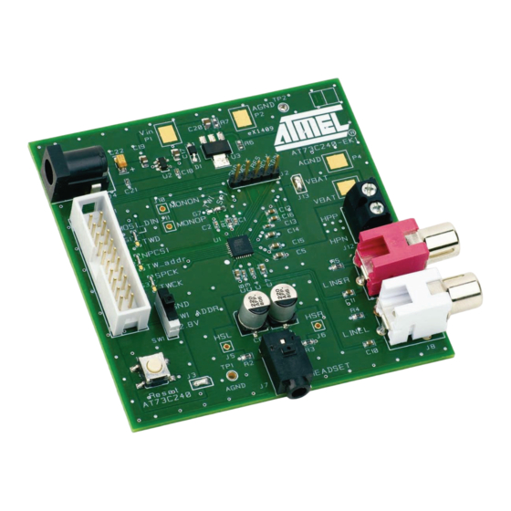
– I²S On-board buttons: – AT73C240 Reset, – SPI/TWI Communication, – TWI Address selection Deliverables The AT73C240-EK1 package contains the following items: An AT73C240-EK1 board, A Parallel-to-Serial board, A DC/DC power supply cable, 20-Lead flat cable, A parallel cable, One CD-ROM containing the product’s software, User Guide and a full Datasheet. - Page 7 Figure 1-1. AT73C240-EK1 Top View (card photo) The AT73C240 is located in the center of the AT73C240-EK1 on the Components Side. Figure 1-2. AT73C240-EK1Card With Available Connections AT73C240-EK1 Evaluation Kit User Guide 6482A–PMAAC–11-Jun-09...
- Page 8 Figure 1-3. AT73C240-EK1 Components Side AT73C240-EK1 Evaluation Kit User Guide 6482A–PMAAC–11-Jun-09...
-
Page 9: Getting Started
Getting Started Electrostatic Warning The AT73C240-EK1 evaluation board is shipped in protective anti-static packaging. The board must not be subjected to high electrostatic potentials. A grounding strap or similar protective device should be connected when handling the board. Avoid touching the components pins or any metallic element. -
Page 10: Instructions
Install «DLPORTIO.exe» from the provided software CD and restart your PC. Install the AT73C240 software by clicking on setup.exe. If the software is downloaded from the Atmel Web site then it is necessary to install first the National Instrument Labview software (LabVIEW8.0.1RuntimeEngine). -
Page 11: Block Diagram
6V to 9V from Parallel-to-Serial 6V to 9V Header AC/DC Transformer Card Min 500mA Min 500mA Power Amplifier AT73C240-EK1 20 Leads Standard Board Flat Cable Parallel Cable Line In (TWI / SPI) Right/Left Headset AT73C240-EK1 Evaluation Kit User Guide 6482A–PMAAC–11-Jun-09... -
Page 12: Power Supply
VBAT 2.7.1 AC/DC Transformer or External Power Supply The transformer is used as the main power source (Vin) for the AT73C240-EK1. Connect it, to J1 of Par- allel-to-serial card (NEB21R type), when using the software. Table 2-1. Transformer Requirements Power supply source... - Page 13 If chosen as an alternative, connect the power supply (+) to Vin pad (P1) and (-) to GND pad (P2). Figure 2-6. Vin Supply Pad (P1) Vin (6V to 9V) J13 - VBAT Jumper (Connect an Ampermeter in serial for current measuer- ments) AT73C240-EK1 Evaluation Kit User Guide 6482A–PMAAC–11-Jun-09...
-
Page 14: Supply With A Power Supply On Audio Power Amplifier
The on board supply voltage “grain-cafe“ (G4, G5, & G6 located on the print-side of the board - layer 2) enable correct connection between the Power Supply and the AT73C240. Keep these jumpers closed or open them for current measurements (see Figure 2-18 on page 2-13). Figure 2-8. On Board Supply Jumpers AT73C240-EK1 Evaluation Kit User Guide 6482A–PMAAC–11-Jun-09... -
Page 15: Communication Interfaces
I²S B-clock SPI_DOUT_MISO SPI Data out Not Used TWI Data Note: 1. The I²S signals are independent. They are connected to the Serial Interface Header but not to the level-shifter on the Parallel-to-Serial card. AT73C240-EK1 Evaluation Kit User Guide 6482A–PMAAC–11-Jun-09... -
Page 16: Spi Setup
(for soldering instructions see Figure 2-19 on page 2-13): G1, G2, G3 pads 1 and 2 are soldered G7 pads 2 and 3 are soldered Figure 2-10. SPI Setup 1 2 3 AT73C240-EK1 Evaluation Kit User Guide 6482A–PMAAC–11-Jun-09... -
Page 17: Twi Setup
G1, G2, G3 pads 2 and 3 are soldered, G7 pads 1 and 2 are soldered. Figure 2-11. TWI Setup 1 2 3 TWI Address Figure 2-12. TWI Address Switch (SW1) - Case Address = 0 1 2 3 TWI Address 0x1A AT73C240-EK1 Evaluation Kit User Guide 6482A–PMAAC–11-Jun-09... -
Page 18: I²S Extension Header
Pin N° 1 - GND. Pin N° 2 - MCLK. Pin N° 3 - LRFS. Pin N° 4 - BCLK. Pin N° 5 - SDIN. Figure 2-14. I²S Serial Header (J2) I2S Connector Serial Interface Header 2-10 AT73C240-EK1 Evaluation Kit User Guide 6482A–PMAAC–11-Jun-09... -
Page 19: Audio Interfaces
Negative Output Note: By default the MONON and MONOP outputs are looped to PAIN pins (see Figure 7-1 on page 7-1 ). If needed these signals can be monitored on J10 and J11. AT73C240-EK1 Evaluation Kit User Guide 2-11 6482A–PMAAC–11-Jun-09... - Page 20 2.9.2.1 Line Inputs A line stereo signal can be sent through RCA connectors J8 (Left) and J9 (Right). Figure 2-17. Line Input (J8 & J9) Line In Right Line In Left 2-12 AT73C240-EK1 Evaluation Kit User Guide 6482A–PMAAC–11-Jun-09...
-
Page 21: General Configuration
2.10.1 Configuration Pads A configuration pad configures the AT73C240-EK1 Evaluation Board for custom application. The config- uration is programmable by soldering a specific part of the configuration pad. To return to the initial configuration, the customer has to solder a short jumper. - Page 22 2-14 AT73C240-EK1 Evaluation Kit User Guide 6482A–PMAAC–11-Jun-09...
-
Page 23: Parallel-To-Serial Card
– Adjustable 1.8V to 3.9V output voltage (1A max) – Fixed 3.3V output voltage (100mA max), – 3 power identification leds. Serial interfaces: – Bidirectional buffered Parallel to SPI, – Bidirectional buffered Parallel to TWI. On-board buttons: – Vpad Selection. AT73C240-EK1 Evaluation Kit User Guide 6482A–PMAAC–11-Jun-09... -
Page 24: Parallel-To-Serial Card Components Placement
5. An output DC power source: – Transformer 6V to 9V DC max (minimum 500 mA is required) or, – External power supply connected to Vin pad. 6. PC station with a 25 pins parallel connector. AT73C240-EK1 Evaluation Kit User Guide 6482A–PMAAC–11-Jun-09... -
Page 25: Instructions
Operating power supplied directly from the AC/DC transformer; there is no ON/OFF switch. All data signals from and to the PC are passed straight through. 3.5.2 To turn off the Parallel-to-Serial card evaluation board Disconnect the chosen power supply. AT73C240-EK1 Evaluation Kit User Guide 6482A–PMAAC–11-Jun-09... -
Page 26: Block Diagram
3.3V Pin 6 Regulator 20 Pins Transformer To Buffers 6V to 9V Header (PC side) Regulator Vout_adj Pin 2 Regulator Pin 10 Ground Test points Vin_pad To Buffers Vpad (GPIO Side) AT73C240-EK1 Evaluation Kit User Guide 6482A–PMAAC–11-Jun-09... -
Page 27: Ac/Dc Transformer
Figure 3-5. AC/DC Connector (J1) Input Voltage Front View Side View Input Voltage If chosen as an alternative, connect the power supply (+) to Vin test-point (TP1) and (-) to GND tset- point(TP2 or TP3). AT73C240-EK1 Evaluation Kit User Guide 6482A–PMAAC–11-Jun-09... - Page 28 Vin Supply Test-Points On the Parallel-to-Serial card 3 leds indicate voltage present: D1 - Adjustable Output Voltage D2 - +3.3V D3 - +5V Figure 3-7. Voltages identification Leds Vout_ Adj Led +5V Led +3.3V Led AT73C240-EK1 Evaluation Kit User Guide 6482A–PMAAC–11-Jun-09...
-
Page 29: Vpad Supply Option
Vpad Supplied By On Board 3.3V SW2 is in VO_adj/+3V3 position. SW1 is in +3V3 position. Figure 3-10. Vpad Supplied By Board Adjustable Voltage SW2 is in VO_adj/+3V3 position. SW1 is in VO_adj position. AT73C240-EK1 Evaluation Kit User Guide 6482A–PMAAC–11-Jun-09... -
Page 30: Adjustable Output Voltage
The Parallel-to-Serial card is able to supply up to 1A adjustable output voltage (Vout_adj = 1.8V to 3.9V) for powering an extended card. Vout_adj output level is trimmed by R1 and Its output pin is located on pin N° 2 on J3 header. Figure 3-11. Vout_adj Trimmer (R1) Adjustable Voltage Trimmer AT73C240-EK1 Evaluation Kit User Guide 6482A–PMAAC–11-Jun-09... -
Page 31: Communication Interfaces
2. Input Data - An input signal from supported card to parallel port. 3. Ground - These pins must be connected between the Parallel-to-Serial card and the supported board. 4. Output current is determinate by the limitation of the ACDC transformer. AT73C240-EK1 Evaluation Kit User Guide 6482A–PMAAC–11-Jun-09... -
Page 32: 12.288 Mhz Clock
G7 Open clock on G7 Closed clock off 3.8.3 On Board Configuration Pads The “Grain-cafe” G1 to G5 are not soldered by default. Simply solder it if these signal should be con- nected to the buffers. 3-10 AT73C240-EK1 Evaluation Kit User Guide 6482A–PMAAC–11-Jun-09... -
Page 33: At73C240-Ek1 Software Interface
Software Panel Figure 4-1. Software Panel - General Purpose Page Line In DAC Master DAC Line Out Headset Control Control Control Control Exit Program Automatic Control Power Amplifier DAC Mixer Control DAC Miscellaneous Control AT73C240-EK1 Evaluation Kit User Guide 6482A–PMAAC–11-Jun-09... - Page 34 Resetting all the registers done by pressing once on the AT73C240 Reset push-button I2. In the next read action the registers will be at their default values. Figure 4-3. Reset AT73C240 Button Reset AT73C240 AT73C240-EK1 Evaluation Kit User Guide 6482A–PMAAC–11-Jun-09...
-
Page 35: Technical Specifications
System Unit: Parallel-to-Serial card – Physical Dimensions.................... L= 60 x W=85 x H=20 mm – Weight.................................50 g Operating Conditions 500 mA – External Voltage Supply (From AC/DC Transformer)............6V - 9V/ Connections – Communication Connector....................2x10 pins Header AT73C240-EK1 Evaluation Kit User Guide 6482A–PMAAC–11-Jun-09... - Page 36 AT73C240-EK1 Evaluation Kit User Guide 6482A–PMAAC–11-Jun-09...
-
Page 37: Pcb Layout
Section 6 PCB Layout AT73C240-EK1 Figure 6-1. Layer 1 - Components Layer Note: Size not to scale AT73C240-EK1 Evaluation Kit User Guide 6482A–PMAAC–11-Jun-09... - Page 38 Figure 6-2. Layer 2 Note: Size not to scale AT73C240-EK1 Evaluation Kit User Guide 6482A–PMAAC–11-Jun-09...
-
Page 39: Parallel-To-Serial Card
Parallel-to-Serial Card Figure 6-3. Layer 1 - Components Layer Note: Size not to scale AT73C240-EK1 Evaluation Kit User Guide 6482A–PMAAC–11-Jun-09... - Page 40 Figure 6-4. Layer 2 Note: Size not to scale AT73C240-EK1 Evaluation Kit User Guide 6482A–PMAAC–11-Jun-09...
-
Page 41: Schematics
Section 7 Schematics Figure 7-1. AT73C240-EK1 Schematic AT73C240-EK1 Evaluation Kit User Guide 6482A–PMAAC–11-Jun-09... - Page 42 Figure 7-2. Parallel-to-Serial Card Schematic AT73C240-EK1 Evaluation Kit User Guide 6482A–PMAAC–11-Jun-09...
-
Page 43: Revision History
Section 8 Revision History Revision History Table 8-1. Revision History Document Comments Change Request Ref. 6482A First Issue, 15-May-2009 AT73C240-EK1 Evaluation Kit User Guide 6482A–PMAAC–11-Jun-09... - Page 44 AT73C240-EK1 Evaluation Kit User Guide 6482A–PMAAC–11-Jun-09...
- Page 45 Disclaimer: The information in this document is provided in connection with Atmel products. No license, express or implied, by estoppel or otherwise, to any intellectual property right is granted by this document or in connection with the sale of Atmel products. EXCEPT AS SET FORTH IN ATMEL’S TERMS AND CONDI- TIONS OF SALE LOCATED ON ATMEL’S WEB SITE, ATMEL ASSUMES NO LIABILITY WHATSOEVER AND DISCLAIMS ANY EXPRESS, IMPLIED OR STATUTORY...
- Page 46 AT73C240-EK1 Evaluation Kit User Guide 6482A–PMAAC–11-Jun-09...
Need help?
Do you have a question about the AT73C240-EK1 and is the answer not in the manual?
Questions and answers