
Related Manuals for iWave iW-RainboW-G57D


Summary of Contents for iWave iW-RainboW-G57D
- Page 1 Versal Al Edge SOM DevKit Hardware User Guide iW-RainboW-G57D Versal Al Edge SOM Development Platform Hardware User Guide REL0.4 iWave Systems Technologies Pvt. Ltd. Page 1 of 64...
- Page 2 If you are not the intended recipient (or authorized to receive for the recipient), you are hereby notified that any disclosure, copying distribution or use of any of the information contained within this document is STRICTLY PROHIBITED. Thank you. “iWave Systems Tech. Pvt. Ltd.” REL0.4 iWave Systems Technologies Pvt.
- Page 3 No warranty of accuracy is given concerning the contents of the information contained in this publication. To the extent permitted by law no liability (including liability to any person by reason of negligence) will be accepted by iWave Systems, its subsidiaries or employees for any direct or indirect loss or damage caused by omissions from or inaccuracies in this document.
-
Page 4: Table Of Contents
OWER UTPUT PECIFICATION 3.3 E ......................... 60 NVIRONMENTAL HARACTERISTICS 3.3.1 Environmental Specification ........................60 3.3.2 RoHS Compliance ............................60 3.3.3 Electrostatic Discharge ..........................60 3.4 M ..........................61 ECHANICAL HARACTERISTICS REL0.4 iWave Systems Technologies Pvt. Ltd. Page 4 of 64... - Page 5 Versal Al Edge SOM DevKit Hardware User Guide 3.4.1 Carrier Board Mechanical Dimensions ....................... 61 4. ORDERING INFORMATION............................ 63 REL0.4 iWave Systems Technologies Pvt. Ltd. Page 5 of 64...
- Page 6 23 : P ............................... 58 IGURE OWER 24 : C – T ..................61 IGURE ARRIER BOARD ECHANICAL DIMENSION 25 : C – S ..................62 IGURE ARRIER BOARD ECHANICAL DIMENSION REL0.4 iWave Systems Technologies Pvt. Ltd. Page 6 of 64...
- Page 7 ABLE OWER NPUT EQUIREMENT 12 : P ........................59 ABLE OWER UTPUT PECIFICATION 13 : E ........................60 ABLE NVIRONMENTAL PECIFICATION 14 : O ....................... 63 ABLE RDERABLE RODUCT UMBERS REL0.4 iWave Systems Technologies Pvt. Ltd. Page 7 of 64...
-
Page 8: Introduction
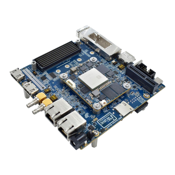
RainboW-G57M-Versal Al Edge-SOM-HardwareUserGuide”. Overview iWave's Versal Al Edge Development platform comes with Versal Al Edge SOM and the REN Carrier Board. The development board can be used for quick prototyping of various applications targeted by the Versal Al Edge. With the 120mm x 120mm size, carrier board is packed with all the necessary on-board connectors to validate the features of Versal Al Edge SOM. - Page 9 Peripheral Module Interface Programmable Logic Processing System RGMII Reduced Gigabit Media Independent Interface Real Time Clock Serial Digital Interface Serial Peripheral Interface UART Universal Asynchronous Receiver Transmitter Universal Serial Bus REL0.4 iWave Systems Technologies Pvt. Ltd. Page 9 of 64...
-
Page 10: References
Note: Signal Type does not include internal pull-ups or pull-downs implemented by the chip vendors and only includes the pull-ups or pull-downs implemented on board. References Versal Al Edge Datasheet & Reference Manual Versal Al Edge SOM Hardware User Guide REL0.4 iWave Systems Technologies Pvt. Ltd. Page 10 of 64... -
Page 11: Architecture And Design
HS Receiver x 3 HDMI IN Connector HS Transmitter x 1 SDI OUT Connector HS Receiver x 1 SDI IN Connector Figure 1: Versal Al Edge SOM Carrier Board Block Diagram REL0.4 iWave Systems Technologies Pvt. Ltd. Page 11 of 64... -
Page 12: Versal Al Edge Som Carrier Board Features
Clock Synthesizers/Generators x2 RTC Coin Cell Holder x 1 Reset Button General Specification Power Supply : DC 12V, 5A Power Input Jack Form Factor : 120mm x 120mm REL0.4 iWave Systems Technologies Pvt. Ltd. Page 12 of 64... - Page 13 (Boot SEL1) (Boot SEL2) Switch Position Image SW4.1 SW4.2 SW4.3 PS JTAG QSPI (Default) Note: In Versal SOM, PS Mode3(4 bit)boot mode signal is connected to Ground through 10K resistors. REL0.4 iWave Systems Technologies Pvt. Ltd. Page 13 of 64...
-
Page 14: Board To Board Connectors
Note: For the Board-to-Board Connector1 pinout, refer the Versal Al Edge SOM Hardware User Guide. Figure 2: Board to Board Connector1 Note: REN Carrier Board is common for our other SOM also. Board to Board connector3 is not applicable for Versal AI Edge SOM. REL0.4 iWave Systems Technologies Pvt. Ltd. Page 14 of 64... -
Page 15: Board To Board Connector2
Figure 3: Board to Board Connector 2 Note: REN Carrier Board is common for our other SOM also. Board to Board connector3 is not applicable for Versal AI Edge SOM. REL0.4 iWave Systems Technologies Pvt. Ltd. Page 15 of 64... -
Page 16: Ps Interface Features
Speed (Yellow) and Link/Activity (Green) LED indications on RJ45 Magjack connector. This RJ45 Magjack connector (J5) is physically located at the top of the board as shown below. Figure 4: Gigabit Ethernet Connector1 REL0.4 iWave Systems Technologies Pvt. Ltd. Page 16 of 64... -
Page 17: Gigabit Ethernet Port2
RJ45 Magjack (J9). Also, it supports Speed (Yellow) and Link/Activity (Green) LED indications on RJ45 Magjack connector. This RJ45 Magjack connector is physically located at the top of the board as shown below. Figure 5: Gigabit Ethernet Connector2 REL0.4 iWave Systems Technologies Pvt. Ltd. Page 17 of 64... -
Page 18: Usb2.0 Otg Port
B2B-2) and controls the power using the USB_PWR_EN pin (B16 pin of B2B-2). This USB2.0 OTG connector (J4) is physically located at the top of the board as shown below. Figure 6: USB OTG Connector REL0.4 iWave Systems Technologies Pvt. Ltd. Page 18 of 64... -
Page 19: Micro Sd Port
1.8V IO level is selected for SD1 signals to SD connector. The Micro SD connector (J3) is physically located at the top of the board as shown below. Figure 7: Micro SD Connector REL0.4 iWave Systems Technologies Pvt. Ltd. Page 19 of 64... -
Page 20: Gpio Header
Board to Board connector 2. These header supports SPI, CAN, and PS GPIOs. These GPIO Header (J19) is physically located at the top of the board as shown below. Figure 8: GPIO Header REL0.4 iWave Systems Technologies Pvt. Ltd. Page 20 of 64... - Page 21 Signal Name Description Termination VCC_5V O, 5V Power 5V Supply Voltage. VCC_5V O, 5V Power 5V Supply Voltage. Power Ground Power Ground Power Ground VCC_1V8 O, 1.8V Power 1V8 Supply Voltage. REL0.4 iWave Systems Technologies Pvt. Ltd. Page 21 of 64...
- Page 22 SPI MOSI. This Pin is connected to D17 pin of Board-to-Board Connector2 (J3). PMC_MIO10_500 SPI_MISO_IO1/Bank3_IO2 I, 1.8V LVCMOS SPI MISO. This Pin is connected to D18 pin of Board-to-Board Connector2 (J3). REL0.4 iWave Systems Technologies Pvt. Ltd. Page 22 of 64...
-
Page 23: Usb Type-C For Debug Uart And Jtag
USB D+ (DP) and D- (DM) signals directly to the USB Type-C connector. The USB Type-C connector (J8) is located at the top side of the board as shown below. Figure 9: Debug Connector REL0.4 iWave Systems Technologies Pvt. Ltd. Page 23 of 64... -
Page 24: Interface Features
I2C address 0x2D. SDI Video IN HD BNC connector (J14) is physically located at the top of the board as shown below. Note: By default, 12G Adaptive Cable Equalizer chip “LMH1297” is supported on the board. To support 3G Adaptive Cable Equalizer chip “LMH0397”, contact iWave. Figure 10: SDI Video IN REL0.4 iWave Systems Technologies Pvt. -
Page 25: Sdi Video Out
I2C address 0x30. SDI Video OUT HD BNC connector (J13) is physically located at the top of the board as shown below. Note: By default, 12G Adaptive Cable Equalizer chip “LMH1297” is supported on the board. To support 3G Adaptive Cable Equalizer chip “LMH0397”, contact iWave. Figure 11: SDI Video OUT REL0.4 iWave Systems Technologies Pvt. -
Page 26: Hdmi In
Connector (J21) through AC caps for HDMI IN support. HDMI-IN cable detect feature is supported through PL IO through level translator. HDMI IN connector (J21) is physically located at the top of the board as shown below. Figure 12: HDMI IN Connector REL0.4 iWave Systems Technologies Pvt. Ltd. Page 26 of 64... -
Page 27: Hdmi Out
Bank104 Channel0 to Channel2 GTYP transceiver from Board to Board connector2 is directly connected to HDMI Retimer chip (SN65DP159RGZR) through AC caps and then connected to HDMI OUT Connector (J17) for HDMI Video out. Figure 13: HDMI OUT Connector REL0.4 iWave Systems Technologies Pvt. Ltd. Page 27 of 64... -
Page 28: Pmod Host Port Connector
3.3V IO level, the signals from Board-to-Board connector are connected to Pmod Connectors through Voltage level translator. Pmod Host port connector (J22) are physically located at the bottom of the board as shown below. Figure 14: PMOD Host Connector iWave Systems Technologies Pvt. Ltd. REL0.4 Page 28 of 64... - Page 29 General purpose Input Output. IO_L9P_302 BANK2_IO8P IO, 3V3 LVCMOS General purpose Input Output. IO_L8P_302 BANK2_IO7P IO, 3V3 LVCMOS General purpose Input Output. Power Ground. VCC_3V3 O, 3.3V Power 3V3 Supply Voltage. iWave Systems Technologies Pvt. Ltd. REL0.4 Page 29 of 64...
-
Page 30: Fmc+ Hpc Connector
Up to 25 LVDS IOs/50 Single ended (SE) IOs from XPIO Bank 703 This 560Pin FMC+ HPC connector (J20) is physically located at the top of the board as shown below. Figure 15: FMC+ Connector iWave Systems Technologies Pvt. Ltd. REL0.4 Page 30 of 64... - Page 31 * By default, FMC+ connector power is disabled as per Vita Specification. While booting the FMC+ Modules EEPROM is read and enabling the FMC+ connector power. * If FMC+ modules EEPROM is not programmed, then FMC+ connector power is not enabled. iWave Systems Technologies Pvt. Ltd. REL0.4 Page 31 of 64...
- Page 32 DP2_C2M_P GTYP_TXP2_103 GTYP_TXP2_103 O, DIFF Connector 2 differential transmitter positive. GTYP_TXN2_103 GTYP Bank103 channel2 High speed Board to Board DP2_C2M_N GTYP_TXN2_103 O, DIFF Connector 2 differential transmitter negative. Ground. Power REL0.4 iWave Systems Technologies Pvt. Ltd. Page 32 of 64...
- Page 33 Ground. Power Ground. Power DP8_M2C_P DP8_M2C_N Power Ground. Power Ground. DP7_M2C_P DP7_M2C_N Ground. Power Power Ground. DP6_M2C_P DP6_M2C_N Ground. Power Ground. Power GBTCLK1_M2C_P GBTCLK1_M2C_N Ground. Power Ground. Power DP9_C2M_P DP9_C2M_N REL0.4 iWave Systems Technologies Pvt. Ltd. Page 33 of 64...
- Page 34 PL Bank703 IO2 differential positive. LA10_P XP_G27_LVDS703_L2P IO_L2P_N0P4_703 IO, 1.5V Connector 1 Board to Board PL Bank703 IO2 differential negative. LA10_N XP_F28_LVDS703_L2N IO_L2N_N0P5_703 IO, 1.5V Connector 1 Ground. Power Ground. Power REL0.4 iWave Systems Technologies Pvt. Ltd. Page 34 of 64...
- Page 35 3P3V VCC_3V3_FMC+ Power Ground. Power Good Signal from Carrier to FMC+ Module. PG_C2M O, 3.3V This Pin is connected to 8th pin of IO Expander (U52). Ground. Power Ground. Power REL0.4 iWave Systems Technologies Pvt. Ltd. Page 35 of 64...
- Page 36 Board to Board LA26_P XP_L23_LVDS702_L16P IO_L16P_N5P2_M0P140_702 IO, 1.5V PL Bank702 IO16 differential positive. Connector 1 Board to Board PL Bank702 IO16 differential negative. LA26_N XP_K24_LVDS702_L16N IO_L16N_N5P3_M0P141_702 IO, 1.5V Connector 1 Power Ground. REL0.4 iWave Systems Technologies Pvt. Ltd. Page 36 of 64...
- Page 37 Board to Board HA05_P XP_R27_LVDS702_L1P IO_L1P_N0P2_M0P110_702 IO, 1.5V PL Bank702 IO1 differential positive. connector 1 Board to Board PL Bank702 IO1 differential negative. HA05_N XP_T28_LVDS702_L1N IO_L1N_N0P3_M0P111_702 IO, 1.5V connector 1 Ground. Power REL0.4 iWave Systems Technologies Pvt. Ltd. Page 37 of 64...
- Page 38 O, 1.5V Power Carrier Board Supply Voltage. VADJ VCC_FMC+_ADJ Ground. Power Power Good Signal from FMC Module to Carrier. I, 3.3V CMOS/ PG_M2C 10K PU This Pin is connected to 5th pin of IO Expander (U52). REL0.4 iWave Systems Technologies Pvt. Ltd. Page 38 of 64...
- Page 39 Board to Board HA15_P Connector 1 Board to Board HA15_N Connector 1 Ground. Power HA19_P HA19_N Power Ground. HB02_P HB02_N Power Ground. HB04_P HB04_N Ground. Power HB08_P HB08_N Ground. Power HB12_P HB12_N REL0.4 iWave Systems Technologies Pvt. Ltd. Page 39 of 64...
- Page 40 Board to Board LA16_N XP_B25_LVDS703_L9N_GC IO_L9N_GC_XCC_N3P1_703 IO, 1.5V PL Bank703 IO9 differential negative. Connector 1 Ground. Power Board to Board PL Bank703 IO11 differential positive. LA20_P XP_B26_LVDS703_L11P IO_L11P_N3P4_703 IO, 1.5V Connector 1 REL0.4 iWave Systems Technologies Pvt. Ltd. Page 40 of 64...
- Page 41 Board to Board PL Bank702 IO11 differential negative. CLK0_M2C_N XP_K26_LVDS702_L11N IO_L11N_N3P5_M0P131_702 IO, 1.5V Connector 1 Ground. Power Board to Board IO_L18P_XCC_N6P0_703 PL Bank703 IO18 differential positive. LA02_P XP_G21_LVDS703_L18P IO, 1.5V Connector 1 REL0.4 iWave Systems Technologies Pvt. Ltd. Page 41 of 64...
- Page 42 Board to Board LA28_P XP_K27_LVDS702_L5P IO_L5P_N1P4_M0P118_702 IO, 1.5V PL Bank702 IO5 differential positive. Connector 1 Board to Board PL Bank702 IO5 differential negative. LA28_N XP_K28_LVDS702_L5N IO_L5N_N1P5_M0P119_702 IO, 1.5V Connector 1 Ground. Power REL0.4 iWave Systems Technologies Pvt. Ltd. Page 42 of 64...
- Page 43 XP_P22_LVDS702_L20N IO_L20N_N6P5_M0P149_702 IO, 1.5V Connector 1 Ground. Power Board to Board HA14_P Connector 1 Board to Board HA14_N Connector 1 Ground. Power HA18_P HA18_N Ground. Power HA22_P HA22_N Ground. Power REL0.4 iWave Systems Technologies Pvt. Ltd. Page 43 of 64...
- Page 44 Board to Board PL Bank702 IO19 differential positive. HA10_P XP_T21_LVDS702_L19P IO_L19P_N6P2_M0P146_702 IO, 1.5V Connector 1 Board to Board PL Bank702 IO19 differential negative. HA10_N XP_R22_LVDS702_L19N IO_L19N_N6P3_M0P147_702 IO, 1.5V Connector 1 Ground. Power REL0.4 iWave Systems Technologies Pvt. Ltd. Page 44 of 64...
- Page 45 HB10_N Power Ground. HB14_P HB14_N Ground. Power HB17_P_CC HB17_N_CC Ground. Power VIO_B_M2C RES1 Ground. Power Ground. Power GBTCLK4_M2C_P GBTCLK4_M2C_N Ground. Power Ground. Power GBTCLK3_M2C_P GBTCLK3_M2C_N Ground. Power Ground. Power GBTCLK2_M2C_P REL0.4 iWave Systems Technologies Pvt. Ltd. Page 45 of 64...
- Page 46 Carrier Board Supply Voltage. Power Ground. Ground. Power Carrier Board Supply Voltage. 12P0V VCC_12V_FMC+ O, 12V Power Power Ground. DP23_M2C_P DP23_M2C_N Power Ground. Power Ground. DP22_M2C_P DP22_M2C_N Power Ground. Ground. Power DP21_M2C_P DP21_M2C_N REL0.4 iWave Systems Technologies Pvt. Ltd. Page 46 of 64...
- Page 47 DP17_C2M_N Ground. Power Ground. Power DP18_C2M_P DP18_C2M_N Power Ground. Power Ground. DP19_C2M_P DP19_C2M_N Power Ground. Ground. Power DP23_C2M_P DP23_C2M_N Power Ground. Ground. Power DP21_C2M_P DP21_C2M_N Ground. Power Ground. Power DP10_M2C_P REL0.4 iWave Systems Technologies Pvt. Ltd. Page 47 of 64...
- Page 48 Ground. Power FMC+ Module Present Signal. HSPC_PRSNT_M2C This Pin is connected to 7 pin of IO I,3.3V/10K PU Expander (U52). Ground. Power Ground. Power DP22_C2M_P DP22_C2M_N Ground. Power Ground. Power REL0.4 iWave Systems Technologies Pvt. Ltd. Page 48 of 64...
- Page 49 Note: * FMC+ connector supports VADJ 1.8V, 1.5V and 1.2V. By default, VADJ is set to 1.5V. Contact iWave for further details. *IO Type of IOs originating from Versal Al Edge is configurable. Hence for exact IO type configuration options, refer Xilinx Versal Al Edge datasheet.
-
Page 50: Additional Features
0 of GTYP bank104 OUT9n HS_TXVR1_CLK0N B2B-2 B42 pin. This clock is from OUT9n of Clock synthesizer1. This clock is input to reference clock 0 of GTYP bank104 REL0.4 iWave Systems Technologies Pvt. Ltd. Page 50 of 64... -
Page 51: Figure 18 : Clock Tree
B2B Connector 2 Oscillator1 156.25MHz (HDMI) HDMI RX Connector OUT9P/N TXVR1-REFCLK0 TXVR1-REFCLK1 Clock Synthesizer 2 148.5MHz (SDI) FMC+ Connector OUT0P/N TXVR0-REFCLK1 TXVR0-REFCLK0 CLK_SYNTH2 (100MHz) SI5332 25MHz (Option) Figure 17: Clock Tree REL0.4 iWave Systems Technologies Pvt. Ltd. Page 51 of 64... -
Page 52: Io Expanders
For BOM Configuration 10K PD I, 3.3V CMOS/ IOEXP1_BRD_CONFIG4 For BOM Configuration 10K PD I, 3.3V CMOS/ IOEXP1_BRD_CONFIG5 For BOM Configuration 10K PD I, 3.3V CMOS/ IOEXP1_BRD_CONFIG6 For BOM Configuration 10K PD REL0.4 iWave Systems Technologies Pvt. Ltd. Page 52 of 64... - Page 53 Connected to FMC+ Power sequence control B_FMC+_12V_EN 10K PD O, 3.3V CMOS/ Connected to FMC+ Power sequence control B_FMC+_3V3_EN 10K PD O, 3.3V CMOS/ Connected to FMC+ Regulator B_FMC+_ADJ_EN 10K PD REL0.4 iWave Systems Technologies Pvt. Ltd. Page 53 of 64...
-
Page 54: I2C Tree
0x22h I2C MUX USB Controller 0x5Bh 0x71h HDMI Retimer I2C0_MUX1 0x21h IO Expander 2 0x2Dh SDI IN 0x30h SDI OUT I2C0_MUX2 0x50h FMC+ Connector 0x50h EEPROM Figure 18: I2C Tree REL0.4 iWave Systems Technologies Pvt. Ltd. Page 54 of 64... -
Page 55: Power On/Off Switch
The Versal Al Edge Carrier board has power ON/OFF switch (SW1) to control the Main power Input ON/OFF functionality. This power ON/OFF switch is physically located at the top of the board as shown below. Figure 19: Power On/Off Switch REL0.4 iWave Systems Technologies Pvt. Ltd. Page 55 of 64... -
Page 56: Reset Switch
Board-to-Board connector2 Pin B11 is directly connected from Reset Push button switch. This Reset Push button switch (SW5) is physically located at the top of the board as shown below. Figure 20: Reset Switch REL0.4 iWave Systems Technologies Pvt. Ltd. Page 56 of 64... -
Page 57: Rtc Coin Cell Holder
Versal Al Edge SOM for RTC back up voltage when VCC main power is off. This Coin Cell Holder (J23) is physically located at the bottom of the board as shown below. Figure 21: RTC Coin Cell Holder REL0.4 iWave Systems Technologies Pvt. Ltd. Page 57 of 64... -
Page 58: Technical Specification
12V power input from an external power supply is connected to the Versal Al Edge Carrier Board through Power Jack (J2). This connector is physically placed at the top of the board as shown below. Figure 22: Power Jack REL0.4 iWave Systems Technologies Pvt. Ltd. Page 58 of 64... -
Page 59: Power Output Specification
3.45 3P3VAUX 3.15 3.45 100mA VCC_12V 11.75V 12.25V To Pmod Connector VCC_3V3 3.15 3.45 100mA To GPIO Header VCC_5V 4.85V 5.15V 500mA VCC_1V8 1.75 1.85 100mA VIO_BANK2 1.75 1.85 100mA REL0.4 iWave Systems Technologies Pvt. Ltd. Page 59 of 64... -
Page 60: Environmental Characteristics
3.3.3 Electrostatic Discharge iWave’s Versal Al Edge SOM Development platform is sensitive to electrostatic discharge and so high voltages caused by static electricity could damage some of the devices on board. It is packed with necessary protection while shipping. -
Page 61: Mechanical Characteristics
3.4.1 Carrier Board Mechanical Dimensions The REN Carrier board PCB form factor is 120mm x 120mm and Board mechanical dimension is shown below. Figure 23: Carrier board Mechanical dimension – Top View REL0.4 iWave Systems Technologies Pvt. Ltd. Page 61 of 64... - Page 62 Connector (14.75mm) and bottom side maximum height component is CMC (9.32mm). Please refer the below figure for height details of the Versal Al Edge SOM Carrier board. Figure 24: Carrier board Mechanical dimension – Side View REL0.4 iWave Systems Technologies Pvt. Ltd. Page 62 of 64...
-
Page 63: Table 14 : Orderable Product
Versal Al Edge SOM and Carrier Board. Table 14: Orderable Product Part Numbers Temperature Product Part Number Description Note: For Development platform identification purpose, Product part number is pasted as Label with Barcode readable format. REL0.4 iWave Systems Technologies Pvt. Ltd. Page 63 of 64... - Page 64 Versal Al Edge SOM DevKit Hardware User Guide REL0.4 iWave Systems Technologies Pvt. Ltd. Page 64 of 64...
Need help?
Do you have a question about the iW-RainboW-G57D and is the answer not in the manual?
Questions and answers