Advertisement
Quick Links
This user's guide describes the characteristics, operation, and use of the TPD3S714-Q1EVM evaluation
module (EVM). This EVM includes four
testing.
1. IEC61000-4-2 compliance testing on the connector-side pin
2. 4-port s-parameter analysis
3. USB 2.0 Type A input and output connectors for throughput analysis
4. ESD clamping waveforms during an electrostatic discharge (ESD) event
...................................................................................................................
1
Introduction
.....................................................................................................................
2
Definitions
..........................................................................................................................
3
Setup
4
Board Layout
5
Schematics and Bill Of Materials
1
Ideal Contact Discharge Waveform of the Output Current of the ESD Simulator at 4 kV
2
System Level ESD Test Setup
3
TPD3S714-Q1EVM Top Components and Silkscreen
4
TPD3S714-Q1EVM Top Layer
SLVUAC1B – October 2015 – Revised May 2017
Submit Documentation Feedback
TPD3S714-Q1
................................................................................................................
..........................................................................................
.............................................................................................
.............................................................................................
Copyright © 2015–2017, Texas Instruments Incorporated
SLVUAC1B – October 2015 – Revised May 2017
devices (SLVSCG4) in various configurations for
Contents
List of Figures
..................................................................
User's Guide
TPD3S714-Q1EVM
.........................
TPD3S714-Q1EVM
2
3
4
7
9
3
6
7
7
1
Advertisement

Related Manuals for Texas Instruments TPD3S714-Q1EVM


Summary of Contents for Texas Instruments TPD3S714-Q1EVM
- Page 1 User's Guide SLVUAC1B – October 2015 – Revised May 2017 TPD3S714-Q1EVM This user's guide describes the characteristics, operation, and use of the TPD3S714-Q1EVM evaluation module (EVM). This EVM includes four TPD3S714-Q1 devices (SLVSCG4) in various configurations for testing. 1. IEC61000-4-2 compliance testing on the connector-side pin 2.
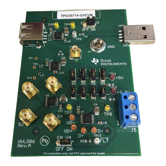
- Page 2 The TPD3S714-Q1 is characterized for operation over an ambient air temperature range of -40°C to 125°C. The TPD3S714-Q1EVM contains four TPD3S714-Q1s labeled U1 through U4. U1 is configured with two USB2.0 Type A connectors (USB1 and USB2) for capturing system level tests. U2 is configured with four SMA (S1 –...
- Page 3 ±30% [A] ±30% [A] 22.5 Figure 1. Ideal Contact Discharge Waveform of the Output Current of the ESD Simulator at 4 kV SLVUAC1B – October 2015 – Revised May 2017 TPD3S714-Q1EVM Submit Documentation Feedback Copyright © 2015–2017, Texas Instruments Incorporated...
- Page 4 SMB (J3) connector for capturing clamping waveforms with an oscilloscope during an ESD strike. Caution must be taken when capturing clamping waveforms during an ESD event so as not to damage the oscilloscope. TPD3S714-Q1EVM SLVUAC1B – October 2015 – Revised May 2017 Submit Documentation Feedback Copyright © 2015–2017, Texas Instruments Incorporated...
- Page 5 Recommended settings for the time axis is 20 ns/div and for the voltage axis is 10 V division. The voltage levels of the ESD applied to TP2. should not exceed ± 8 kV while capturing clamping waveforms. SLVUAC1B – October 2015 – Revised May 2017 TPD3S714-Q1EVM Submit Documentation Feedback Copyright © 2015–2017, Texas Instruments Incorporated...
- Page 6 J5.3 is V . Kelvin connections (TP7 and TP8) are provided for accurate voltage measurements of BUS_CON and V under load tests. BUS_SYS BUS_CON TPD3S714-Q1EVM SLVUAC1B – October 2015 – Revised May 2017 Submit Documentation Feedback Copyright © 2015–2017, Texas Instruments Incorporated...
- Page 7 Board Layout www.ti.com Board Layout This section provides the TPD3S714-Q1EVM board layout. TPD3S714-Q1EVM is a 4-layer board of FR-4 at 0.062” thickness. Layers 2 and 3 are power planes and not shown here. Figure 3. TPD3S714-Q1EVM Top Components and Silkscreen Figure 4.
- Page 8 Board Layout www.ti.com Figure 5. TPD3S714-Q1EVM Bottom Layer TPD3S714-Q1EVM SLVUAC1B – October 2015 – Revised May 2017 Submit Documentation Feedback Copyright © 2015–2017, Texas Instruments Incorporated...
- Page 9 VBUS_CON VBUS_SYS VBUS_CON VBUS_SYS TP10 10µF 100µF TP11 TP12 TP13 10µF TPD3S714-Q1DBQ Copyright © 2017, Texas Instruments Incorporated Figure 6. TPD3S714-Q1EVM Schematic SLVUAC1B – October 2015 – Revised May 2017 TPD3S714-Q1EVM Submit Documentation Feedback Copyright © 2015–2017, Texas Instruments Incorporated...
- Page 10 Schematics and Bill Of Materials www.ti.com TPD3S714-Q1EVM Table 6 illustrates the TPD3S714-Q1EVM bill of materials. Table 6. Bill of Materials Count Designator Description Part Number Manufacturer C1, C4, C7 CAP, CERM, 1 µF, 100 V, +/- 10%, X7S, 0805 C2012X7S2A105K125AB C5, C8, C10, C11 CAP, CERM, 10 µF, 25 V, +/- 10%, X5R, 0805...
- Page 11 NOTE: Page numbers for previous revisions may differ from page numbers in the current version. Changes from A Revision (December 2015) to B Revision ................... Page • Changed TPD3S714-Q1EVM Top Components and Silkscreen to include 2-line common mode choke (CMC) (L5 and ............................L6)............. •...
- Page 12 STANDARD TERMS FOR EVALUATION MODULES Delivery: TI delivers TI evaluation boards, kits, or modules, including any accompanying demonstration software, components, and/or documentation which may be provided together or separately (collectively, an “EVM” or “EVMs”) to the User (“User”) in accordance with the terms set forth herein.
- Page 13 FCC Interference Statement for Class B EVM devices NOTE: This equipment has been tested and found to comply with the limits for a Class B digital device, pursuant to part 15 of the FCC Rules. These limits are designed to provide reasonable protection against harmful interference in a residential installation.
- Page 14 【無線電波を送信する製品の開発キットをお使いになる際の注意事項】 開発キットの中には技術基準適合証明を受けて いないものがあります。 技術適合証明を受けていないもののご使用に際しては、電波法遵守のため、以下のいずれかの 措置を取っていただく必要がありますのでご注意ください。 1. 電波法施行規則第6条第1項第1号に基づく平成18年3月28日総務省告示第173号で定められた電波暗室等の試験設備でご使用 いただく。 2. 実験局の免許を取得後ご使用いただく。 3. 技術基準適合証明を取得後ご使用いただく。 なお、本製品は、上記の「ご使用にあたっての注意」を譲渡先、移転先に通知しない限り、譲渡、移転できないものとします。 上記を遵守頂けない場合は、電波法の罰則が適用される可能性があることをご留意ください。 日本テキサス・イ ンスツルメンツ株式会社 東京都新宿区西新宿6丁目24番1号 西新宿三井ビル 3.3.3 Notice for EVMs for Power Line Communication: Please see http://www.tij.co.jp/lsds/ti_ja/general/eStore/notice_02.page 電力線搬送波通信についての開発キットをお使いになる際の注意事項については、次のところをご覧ください。http:/ /www.tij.co.jp/lsds/ti_ja/general/eStore/notice_02.page 3.4 European Union 3.4.1 For EVMs subject to EU Directive 2014/30/EU (Electromagnetic Compatibility Directive): This is a class A product intended for use in environments other than domestic environments that are connected to a low-voltage power-supply network that supplies buildings used for domestic purposes.
- Page 15 Notwithstanding the foregoing, any judgment may be enforced in any United States or foreign court, and TI may seek injunctive relief in any United States or foreign court. Mailing Address: Texas Instruments, Post Office Box 655303, Dallas, Texas 75265 Copyright © 2017, Texas Instruments Incorporated...
- Page 16 IMPORTANT NOTICE FOR TI DESIGN INFORMATION AND RESOURCES Texas Instruments Incorporated (‘TI”) technical, application or other design advice, services or information, including, but not limited to, reference designs and materials relating to evaluation modules, (collectively, “TI Resources”) are intended to assist designers who are developing applications that incorporate TI products;...
- Page 17 Mouser Electronics Authorized Distributor Click to View Pricing, Inventory, Delivery & Lifecycle Information: Texas Instruments TPD3S714-Q1EVM...
Need help?
Do you have a question about the TPD3S714-Q1EVM and is the answer not in the manual?
Questions and answers