Advertisement
Quick Links
TPD2E1B06DRLEVM
This user's guide describes the characteristics, operation, and use of the TPD2E1B06DRLEVM evaluation
module (EVM). This EVM includes 7 TPD2E1B06DRL's in various configurations for testing. Five
TPD2E1B06DRL's are configured for IEC61000-4-2 compliance testing, one TPD2E1B06DRL is
configured for 4-port s-parameter analysis, and one is configured for throughput on USB 2.0 Type A
connectors for throughput analysis. Additionally, two of the TPD2E1B06DRL's for ESD testing also allow
the capture of clamping waveforms during an ESD event. This user's guide includes setup instructions,
schematic diagrams, a bill of materials, and printed-circuit board layout drawings for the evaluation
module.
1
INTRODUCTION
Texas Instrument's TPD2E1B06DRL evaluation module helps designers evaluate the operation and
performance of the TPD2E1B06DRL device. The TPD2E1B06DRL is a dual channel ESD protection
device in a small DRL package which offers IEC61000-4-2 Level 4 compliant ESD protection. The 1 pF
line capacitance is suitable for a wide range of applications. The TPD2E1B06DRL is characterized for
operation over an ambient air temperature range of -40°C to 125°C.
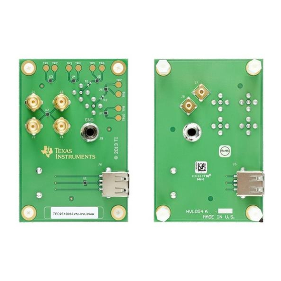
The EVM contains seven TPD2E1B06DRL's. A single TPD2E1B06DRL (U1) is configured with two
USB2.0 Type A female connectors (J5 & J6) for capturing Eye Diagrams. The data lines are connected to
TPD2E1B06DRL's IO protection pins. A single TPD2E1B06DRL (U2) is configured with 4 SMA (J1 – J4)
connectors to allow 4-port analysis with a vector network analyzer. Five TPD2E1B06DRL's (U3 – U7) are
configured with test points for striking ESD to the protection pins, two of those (U5 & U6) also have SMB
(J7 & J8) connectors for capturing clamping waveforms with an oscilloscope during ESD test. Caution
must be taken when capturing clamping waveforms during an ESD event so as not to damage the
oscilloscope. A proper procedure is outlined below in
Reference Designator
U3 – U7
U5 & U6
2
DEFINITIONS
Contact Discharge — a method of testing in which the electrode of the ESD simulator is held in contact
with the device-under-test (DUT).
Air Discharge — a method of testing in which the charged electrode of the ESD simulator approaches
the DUT, and a spark to the DUT actuates the discharge.
ESD simulator — a device that outputs IEC61000-4-2 compliance ESD waveforms shown in
with adjustable ranges shown in
IEC61000-4-2 has 4 classes of protection levels. Classes 1 – 4 are shown in
should be incrementally tested to level 4 as shown in
does not fail at 8kV, testing can continue in 2 kV increments until failure.
SLVU917 – August 2013
Submit Documentation Feedback
Table 1. EVM Configuration
TI Part Number
U1
TPD2E1B06DRL
U2
TPD2E1B06DRL
TPD2E1B06DRL
TPD2E1B06DRL
Table 2
Copyright © 2013, Texas Instruments Incorporated
Section
3.4.
USB 2.0 Eye Diagram
IEC61000-4-2 ESD Tests
ESD Clamping waveforms
and
Table
3.
Table 3
until the point of failure. If the DUT
User's Guide
SLVU917 – August 2013
Configuration
S-parameters
Figure 1
Table
2. Stress tests
TPD2E1B06DRLEVM
1
Advertisement

Related Manuals for Texas Instruments TPD2E1B06DRLEVM


Summary of Contents for Texas Instruments TPD2E1B06DRLEVM
- Page 1 SLVU917 – August 2013 TPD2E1B06DRLEVM This user's guide describes the characteristics, operation, and use of the TPD2E1B06DRLEVM evaluation module (EVM). This EVM includes 7 TPD2E1B06DRL’s in various configurations for testing. Five TPD2E1B06DRL’s are configured for IEC61000-4-2 compliance testing, one TPD2E1B06DRL is configured for 4-port s-parameter analysis, and one is configured for throughput on USB 2.0 Type A...
- Page 2 Eye Diagrams. Using either J5 or J6 as input or output, attach to a USB2.0 compliant Eye Diagram tester setup for the intended application, either transmitter or receiver. TPD2E1B06DRLEVM SLVU917 – August 2013 Submit Documentation Feedback Copyright © 2013, Texas Instruments Incorporated...
- Page 3 While the simulator is in direct contact with the test point during contact, it is not during air-gap. Figure 2. System Level ESD Test Setup SLVU917 – August 2013 TPD2E1B06DRLEVM Submit Documentation Feedback Copyright © 2013, Texas Instruments Incorporated...
- Page 4 SMB cable to J8. The voltage levels of the ESD applied to TP5 & TP8 should not exceed +/- 8 kV while capturing clamping waveforms. TPD2E1B06DRLEVM SLVU917 – August 2013 Submit Documentation Feedback Copyright © 2013, Texas Instruments Incorporated...
-
Page 5: Board Layout
BOARD LAYOUT www.ti.com BOARD LAYOUT This section provides the TPD2E1B06DRLEVM board layout. TPD2E1B06DRLEVM is a 4-layer board of FR-4 at 0.062” thickness. Layers 2 and 3 are ground planes and not shown here. Figure 3. TPD2E1B06DRLEVM Top Layer SLVU917 – August 2013... - Page 6 BOARD LAYOUT www.ti.com Figure 4. TPD2E1B06DRLEVM Bottom Layer TPD2E1B06DRLEVM SLVU917 – August 2013 Submit Documentation Feedback Copyright © 2013, Texas Instruments Incorporated...
-
Page 7: Schematics And Bill Of Materials
USB,TYPE A Female J7-8 Conn SMB Jack Str 0.236 X 0.236 inch 131-3701-261 Molex 50 Ohm Pcb Standard Banana 0.312” diameter 575-4 Keystone Jack, Uninsulated, 5.5mm SLVU917 – August 2013 TPD2E1B06DRLEVM Submit Documentation Feedback Copyright © 2013, Texas Instruments Incorporated... -
Page 8: Regulatory Compliance Information
Any exceptions to this are strictly prohibited and unauthorized by Texas Instruments unless user has obtained appropriate experimental/development licenses from local regulatory authorities, which is responsibility of user including its acceptable authorization. - Page 9 FCC Interference Statement for Class B EVM devices This equipment has been tested and found to comply with the limits for a Class B digital device, pursuant to part 15 of the FCC Rules. These limits are designed to provide reasonable protection against harmful interference in a residential installation. This equipment generates, uses and can radiate radio frequency energy and, if not installed and used in accordance with the instructions, may cause harmful interference to radio communications.
- Page 10 Also, please do not transfer this product, unless you give the same notice above to the transferee. Please note that if you could not follow the instructions above, you will be subject to penalties of Radio Law of Japan. Texas Instruments Japan Limited (address) 24-1, Nishi-Shinjuku 6 chome, Shinjuku-ku, Tokyo, Japan http://www.tij.co.jp...
- Page 11 FDA Class III or similar classification, then you must specifically notify TI of such intent and enter into a separate Assurance and Indemnity Agreement. Mailing Address: Texas Instruments, Post Office Box 655303, Dallas, Texas 75265 Copyright © 2013, Texas Instruments Incorporated...
- Page 12 IMPORTANT NOTICE Texas Instruments Incorporated and its subsidiaries (TI) reserve the right to make corrections, enhancements, improvements and other changes to its semiconductor products and services per JESD46, latest issue, and to discontinue any product or service per JESD48, latest issue.
Need help?
Do you have a question about the TPD2E1B06DRLEVM and is the answer not in the manual?
Questions and answers