Advertisement
Quick Links
TPD2E2U06-Q1EVM
This user's guide describes the characteristics, operation, and use of the TPD2E2U06-Q1EVM evaluation
module (EVM). This EVM includes 7 TPD2E2U06-Q1's in various configurations for testing. Five
TPD2E2U06-Q1's are configured for IEC61000-4-2 compliance testing, one TPD2E2U06-Q1 is configured
for 4-port s-parameter analysis, and one is configured for throughput with USB 2.0 Type A connectors.
Additionally, one of the TPD2E2U06-Q1's for ESD testing also allows the capture of a clamping waveform
during an ESD event. This user's guide includes setup instructions, schematic diagrams, a bill of
materials, and printed-circuit board layout drawings for the evaluation module.
1
Introduction
Texas Instrument's TPD2E2U06-Q1 evaluation module helps designers evaluate the operation and
performance of the TPD2E2U06-Q1 device. The TPD2E2U06-Q1 is a dual channel ESD protection device
in a small DBZ package which offers IEC61000-4-2 Level 4 compliant ESD protection. The 1.5 pF line
capacitance is suitable for a wide range of applications. The TPD2E2U06-Q1 is characterized for
operation over an ambient air temperature range of -40°C to 125°C.
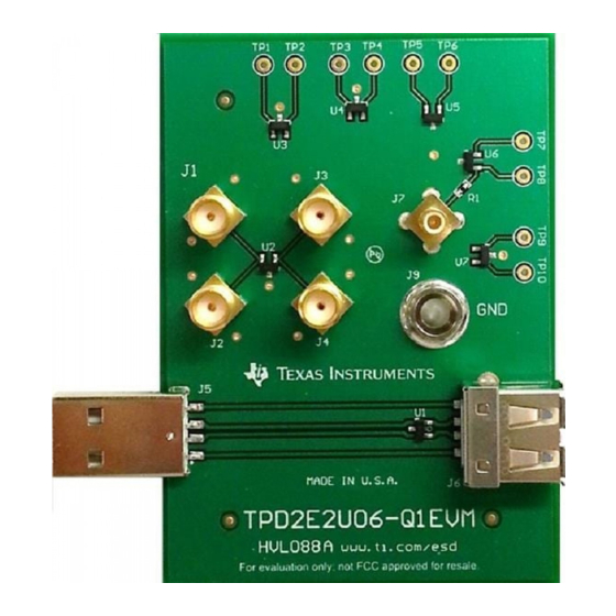
The EVM contains seven TPD2E2U06-Q1's. A single TPD2E2U06-Q1 (U1) is configured with two USB2.0
Type A female connectors (J5 & J6) for capturing Eye Diagrams. The data lines are connected to
TPD2E2U06-Q1's IO protection pins. A single TPD2E2U06-Q1 (U2) is configured with 4 SMA (J1 – J4)
connectors to allow 4-port analysis with a vector network analyzer. Five TPD2E2U06-Q1's (U3 – U7) are
configured with test points for striking ESD to the protection pins, one of those (U6) also has an SMB (J7)
connector for capturing clamping waveforms with an oscilloscope during an ESD strike. Caution must be
taken when capturing clamping waveforms during an ESD event so as not to damage the oscilloscope. A
proper procedure is outlined below in
Reference Designator
U3 – U7
2
DEFINITIONS
Contact Discharge — a method of testing in which the electrode of the ESD simulator is held in contact
with the device-under-test (DUT).
Air Discharge — a method of testing in which the charged electrode of the ESD simulator approaches
the DUT, and a spark to the DUT actuates the discharge.
ESD simulator — a device that outputs IEC61000-4-2 compliance ESD waveforms shown in
with adjustable ranges shown in
IEC61000-4-2 has 4 classes of protection levels. Classes 1 – 4 are shown in
should be incrementally tested to level 4 as shown in
does not fail at 8 kV, testing can continue in 2 kV increments until failure.
SLVUAC6 – December 2014
Submit Documentation Feedback
Section
Table 1. EVM Configuration
TI Part Number
U1
TPD2E2U06-Q1
U2
TPD2E2U06-Q1
TPD2E2U06-Q1
U6
TPD2E2U06-Q1
Table 2
Copyright © 2014, Texas Instruments Incorporated
3.4.
USB 2.0 Eye Diagram
IEC61000-4-2 ESD Tests
ESD Clamping waveforms
and
Table
3.
Table 3
until the point of failure. If the DUT
User's Guide
SLVUAC6 – December 2014
Configuration
S-parameters
Figure 1
Table
2. Stress tests
TPD2E2U06-Q1EVM
1
Advertisement

Related Manuals for Texas Instruments TPD2E2U06-Q1EVM


Summary of Contents for Texas Instruments TPD2E2U06-Q1EVM
- Page 1 SLVUAC6 – December 2014 TPD2E2U06-Q1EVM This user's guide describes the characteristics, operation, and use of the TPD2E2U06-Q1EVM evaluation module (EVM). This EVM includes 7 TPD2E2U06-Q1’s in various configurations for testing. Five TPD2E2U06-Q1’s are configured for IEC61000-4-2 compliance testing, one TPD2E2U06-Q1 is configured for 4-port s-parameter analysis, and one is configured for throughput with USB 2.0 Type A connectors.
- Page 2 Eye Diagrams. Using either J5 or J6 as input or output, attach to a USB2.0 compliant Eye Diagram tester setup for the intended application, either transmitter or receiver. TPD2E2U06-Q1EVM SLVUAC6 – December 2014 Submit Documentation Feedback Copyright © 2014, Texas Instruments Incorporated...
- Page 3 While the simulator is in direct contact with the test point during contact, it is not during air-gap. Figure 2. System Level ESD Test Setup SLVUAC6 – December 2014 TPD2E2U06-Q1EVM Submit Documentation Feedback Copyright © 2014, Texas Instruments Incorporated...
- Page 4 Recommended settings for the time axis is 20 ns/div and for the voltage axis is 10 V division. The voltage levels of the ESD applied to TP8 should not exceed ± 8 kV while capturing clamping waveforms. TPD2E2U06-Q1EVM SLVUAC6 – December 2014 Submit Documentation Feedback Copyright © 2014, Texas Instruments Incorporated...
-
Page 5: Board Layout
Board Layout www.ti.com Board Layout This section provides the TPD2E2U06-Q1EVM board layout. TPD2E2U06-Q1EVM is a 4-layer board of FR-4 at 0.062” thickness. Layers 2, 3 and 4 are identical. Figure 3. TPD2E2U06-Q1EVM Top Layer SLVUAC6 – December 2014 TPD2E2U06-Q1EVM Submit Documentation Feedback... - Page 6 Board Layout www.ti.com Figure 4. TPD2E2U06-Q1EVM Midlayer 1, Midlayer 2, and Bottom Layers TPD2E2U06-Q1EVM SLVUAC6 – December 2014 Submit Documentation Feedback Copyright © 2014, Texas Instruments Incorporated...
-
Page 7: Schematics And Bill Of Materials
Schematics and Bill Of Materials www.ti.com Schematics and Bill Of Materials Schematics Figure 5. TPD2E2U06-Q1EVM Schematic SLVUAC6 – December 2014 TPD2E2U06-Q1EVM Submit Documentation Feedback Copyright © 2014, Texas Instruments Incorporated... - Page 8 Conn SMB Jack Str 50 Ohm Pcb 0.236 X 0.236 inch 131-3701-261 Molex Standard Banana Jack, Uninsulated, 0.312” diameter 575-4 Keystone 5.5mm RES, 150, 5%, 0.063 W, 0402 0402 CRCW0402150RJNED Vishay-Dale TPD2E2U06-Q1EVM SLVUAC6 – December 2014 Submit Documentation Feedback Copyright © 2014, Texas Instruments Incorporated...
- Page 9 STANDARD TERMS AND CONDITIONS FOR EVALUATION MODULES Delivery: TI delivers TI evaluation boards, kits, or modules, including any accompanying demonstration software, components, or documentation (collectively, an “EVM” or “EVMs”) to the User (“User”) in accordance with the terms and conditions set forth herein. Acceptance of the EVM is expressly subject to the following terms and conditions.
- Page 10 FCC Interference Statement for Class B EVM devices NOTE: This equipment has been tested and found to comply with the limits for a Class B digital device, pursuant to part 15 of the FCC Rules. These limits are designed to provide reasonable protection against harmful interference in a residential installation.
- Page 11 【無線電波を送信する製品の開発キットをお使いになる際の注意事項】 本開発キットは技術基準適合証明を受けておりません。 本製品のご使用に際しては、電波法遵守のため、以下のいずれかの措置を取っていただく必要がありますのでご注意ください。 1. 電波法施行規則第6条第1項第1号に基づく平成18年3月28日総務省告示第173号で定められた電波暗室等の試験設備でご使用 いただく。 2. 実験局の免許を取得後ご使用いただく。 3. 技術基準適合証明を取得後ご使用いただく。 なお、本製品は、上記の「ご使用にあたっての注意」を譲渡先、移転先に通知しない限り、譲渡、移転できないものとします。 上記を遵守頂けない場合は、電波法の罰則が適用される可能性があることをご留意ください。 日本テキサス・インスツルメンツ株式会社 東京都新宿区西新宿6丁目24番1号 西新宿三井ビル 3.3.3 Notice for EVMs for Power Line Communication: Please see http://www.tij.co.jp/lsds/ti_ja/general/eStore/notice_02.page 電力線搬送波通信についての開発キットをお使いになる際の注意事項については、次のところをご覧くださ い。http://www.tij.co.jp/lsds/ti_ja/general/eStore/notice_02.page SPACER EVM Use Restrictions and Warnings: 4.1 EVMS ARE NOT FOR USE IN FUNCTIONAL SAFETY AND/OR SAFETY CRITICAL EVALUATIONS, INCLUDING BUT NOT LIMITED TO EVALUATIONS OF LIFE SUPPORT APPLICATIONS.
- Page 12 Notwithstanding the foregoing, any judgment may be enforced in any United States or foreign court, and TI may seek injunctive relief in any United States or foreign court. Mailing Address: Texas Instruments, Post Office Box 655303, Dallas, Texas 75265 Copyright © 2014, Texas Instruments Incorporated...
-
Page 13: Important Notice
IMPORTANT NOTICE Texas Instruments Incorporated and its subsidiaries (TI) reserve the right to make corrections, enhancements, improvements and other changes to its semiconductor products and services per JESD46, latest issue, and to discontinue any product or service per JESD48, latest issue.
Need help?
Do you have a question about the TPD2E2U06-Q1EVM and is the answer not in the manual?
Questions and answers