Table of Contents
Advertisement
Quick Links
User's Guide
May 2, 2002
SN65LV1021/SN65LV1212- SN65LV1023/SN65LV1224
10:1 Serializer/Deserializer Evaluation Board (EVM)
ABSTRACT
This application report focuses the use and construction of a Serializer/Deserializer evaluation module
(EVM) constructed to evaluate the characteristics of SN65LV1021/SN65LV1212 Serializers, and
SN65LV1023/SN65LV1224 Deserializer devices. This document provides guidance on proper use by
showing possible device configurations and test modes. It also provides design, layout, and schematic
information, including specific construction recommendations. Information in this guide can be used to
assist the customer in choosing the optimal design methods and materials in designing a complete
system.
1
SLLU193 - May 2002
11/06/09
Advertisement
Table of Contents

Related Manuals for Texas Instruments SN65LV1021


Summary of Contents for Texas Instruments SN65LV1021
- Page 1 ABSTRACT This application report focuses the use and construction of a Serializer/Deserializer evaluation module (EVM) constructed to evaluate the characteristics of SN65LV1021/SN65LV1212 Serializers, and SN65LV1023/SN65LV1224 Deserializer devices. This document provides guidance on proper use by showing possible device configurations and test modes. It also provides design, layout, and schematic information, including specific construction recommendations.
-
Page 2: Table Of Contents
User's Guide May 2, 2002 TABLE OF CONTENTS EVM DESCRIPTION ..............................3 Figure 1- B LINK Evaluation Board Block Diagram..................4 Board Configuration..............................4 EVM Board Preparation .............................. 5 Figure 2- B LINK EVM Default Jumpers Setup ....................5 Figure 3 – Deserializer-Serializer Interconnect Detail ..................5 Table 1- Jumpers Installation Table ........................ -
Page 3: Evm Description
EVM DESCRIPTION The BLINK EVM provides a vehicle to evaluate the operation and conduct characterization measurements of Texas Instruments SN65LVDS1021/1023 Serializer and SN65LVDS1212/1224 Deserializer devices. The board is setup to permit the independent evaluation of either Serializer or Deserializer devices through the use of external equipment to match the requirements of each device. -
Page 4: Board Configuration
User's Guide May 2, 2002 REFCLK SERDES OUTPUT SERDES INPUT SMA / RJ45 SMA / RJ45 SELECT Select DESERIALIZER SERIALIZER Parallel Parallel outputs Inputs RJ-45 Cat 5 RJ-45 Cat 5 SERDES INPUT POWER POWER CONDITION CONDITION 3.3v +/-10% Figure 1- B LINK Evaluation Board Block Diagram Board Configuration The B LINK evaluation board can be configured to permit independent evaluation of either Serializer or Deserializer devices or joined in cooperation with each other as a pair. -
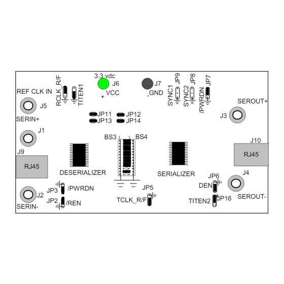
Page 5: Evm Board Preparation
User's Guide May 2, 2002 EVM Board Preparation Prior to applying power to the board verify that jumpers are properly installed as shown in Table 1- Jumpers Installation Table. Figure 2, provides a simplified top view of the EVM that can be used to assist in rapidly locating these jumpers on the board. - Page 6 User's Guide May 2, 2002 Jumper Default Pin # Function Description Installed RCLK_R/F Deserializer’s RCLK strobe edge selection (high selects rising edge) Installed Logic high input enables Deserializer’s parallel output bus and RCLK into Lo-Z states Installed /PWRDN Deserializer Power-down control. Set to high input to maintain device active Installed TCLK_R/F Serializer’s TCLK strobe edge selection (high selects rising edge )
-
Page 7: Power Connections
User's Guide May 2, 2002 Power Connections The B LINK EVM can be powered from an ordinary DC laboratory bench power supply through the assist of a pair of power supply cables with standard plug banana jacks. • Set the power supply at 3.3 Vdc +/- 10% •... -
Page 8: Optional Configurations And Measurements
User's Guide May 2, 2002 CSA8000 8662/4A Freq= 66MHz. 10 Mhz Mod In RF Out Ref Out 3.3V Pulse Generator Trig Out Ch 1 Ch 1 Ext Trig 8E04 Module 8E01 Module 3.3 vdc REF CLK IN SEROUT+ JP11 JP12 SERIN+ JP13 JP14... -
Page 9: Serializer Jitter Measurements
User's Guide May 2, 2002 Serializer Jitter Measurements Patterns can be introduced in several ways to provide input to the serializer. • In the EVM’s default configuration setup, a serial data stream can be provided to create these patterns. • If all the jumper interconnecting the BS3 BS4 headers are removed data and clock can be provided at BS4. -
Page 10: Pc Board Physical Layout Recommendations
User's Guide May 2, 2002 PC Board Physical Layout Recommendations Serializer and De-Serializer devices should be provided with separate analog and digital power planes; these can co-exist within the same PWB layer and share a common ground where the analog and digital ground pins of each device may be joined. -
Page 11: Blink Schematics
User's Guide May 2, 2002 Appendix A BLINK Schematics SLLU193 - May 2002 11/06/09... -
Page 12: Evm Board Design Stackup
User's Guide May 2, 2002 Appendix B EVM Board Design Stackup General Notes: All Fabrication Items must meet or exceed best industry practice. Laminate Material, copper clad GETEK, E Copper weight: 1 oz Finished board thickness 0.060”+/-0.005” Position Accuracy: +/- 0.0015” Warp &... -
Page 13: Evm Board Design - Top & Bottom Silkscreens
User's Guide May 2, 2002 Appendix B (contd) EVM Board Design – Top & Bottom Silkscreens Top Silkscreen Bottom Silkscreen SLLU193 - May 2002 11/06/09... -
Page 14: Evm Board Design - Top Layer- Ground Layer
User's Guide May 2, 2002 Appendix B (contd) EVM Board Design – Top Layer– Ground Layer SLLU193 - May 2002 11/06/09... -
Page 15: Evm Board Design Power Voltage Layers
User's Guide May 2, 2002 Appendix B (contd) EVM Board Design Power Voltage Layers SLLU193 - May 2002 11/06/09... -
Page 16: Evm Board Design - Ground Layer & Bottom Layer
User's Guide May 2, 2002 Appendix B (contd) EVM Board Design – Ground Layer & Bottom Layer SLLU193 - May 2002 11/06/09... -
Page 17: Blink Evm Bom
Resistor, SMD 0402 R603 R5-R7, R13- R17, R44, R45 R0603 R8, R22 R0603 R9, R23 No Resistors Installed SOC-B66-05-04-0 U1 SN65LV1021 SERIALIZER, SN65LVD1021 100-400MB operation. SN65LV1023 SN65LVD1023 400-660Mb Operation SN65LV1212 DESERIALIZER. SN65LVD1212 100-400MB operation. SN65LV1224 SN65LVD1224 400-660Mb Operation *IF SMA Connectors are used for Serial data {R1=0, R3=0, R18=0, R20=0. Do not Install R2, R4, R19 & R21 } PREFERRED CONFIGURATION Else IF RJ45 Connectors are used for Serial data { Do not Install: R1, R3, R18 or R20 . - Page 18 Any exceptions to this are strictly prohibited and unauthorized by Texas Instruments unless user has obtained appropriate experimental/development licenses from local regulatory authorities, which is responsibility of user including its acceptable authorization.
- Page 19 FCC Interference Statement for Class B EVM devices This equipment has been tested and found to comply with the limits for a Class B digital device, pursuant to part 15 of the FCC Rules. These limits are designed to provide reasonable protection against harmful interference in a residential installation. This equipment generates, uses and can radiate radio frequency energy and, if not installed and used in accordance with the instructions, may cause harmful interference to radio communications.
- Page 20 Also, please do not transfer this product, unless you give the same notice above to the transferee. Please note that if you could not follow the instructions above, you will be subject to penalties of Radio Law of Japan. Texas Instruments Japan Limited (address) 24-1, Nishi-Shinjuku 6 chome, Shinjuku-ku, Tokyo, Japan http://www.tij.co.jp...
- Page 21 FDA Class III or similar classification, then you must specifically notify TI of such intent and enter into a separate Assurance and Indemnity Agreement. Mailing Address: Texas Instruments, Post Office Box 655303, Dallas, Texas 75265 Copyright © 2013, Texas Instruments Incorporated...
- Page 22 IMPORTANT NOTICE Texas Instruments Incorporated and its subsidiaries (TI) reserve the right to make corrections, enhancements, improvements and other changes to its semiconductor products and services per JESD46, latest issue, and to discontinue any product or service per JESD48, latest issue.
Need help?
Do you have a question about the SN65LV1021 and is the answer not in the manual?
Questions and answers