Table of Contents
Advertisement
Quick Links
1
Features
•
2-bit Unidirectional Voltage-level translator
•
Breakout board style EVM for prototype and
evaluation
2
EVM Description
The SN74AVC2T244 is a 2-bit voltage level translator. This translator is a single direction voltage
translator, with OE. When the output-enable (OE) input is high, all outputs are placed in the
high-impedance state. The A port is designed to track VCCA. VCCA accepts any supply voltage from 0.9
V to 3.6 V. The B port is designed to track VCCB. VCCB accepts any supply voltage from 0.9 V to 3.6 V.
This allows for low-voltage bidirectional translation between 1-V, 1.2-V, 1.5-V, 1.8-V, 2.5-V and 3.3-V
voltage nodes.
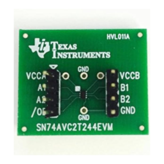
The SN74AVC2T244 EVM was created to allow simplified evaluation and prototyping without the need for
full board development. This EVM provides peripheral header style pads for probing and signal connection
to each device pin. Headers are labeled with the corresponding pin name. The pin number assignments
are given in the following table.
SCEU002 – September 2011
Submit Documentation Feedback
SN74AVC2T244 Evaluation Module
Table 1. Pin Out
1
A
VCCA
B
A1
C
A2
D
OE
Copyright © 2011, Texas Instruments Incorporated
SCEU002 – September 2011
2
VCCB
B1
B2
GND
SN74AVC2T244 Evaluation Module
User's Guide
1
Advertisement
Table of Contents

Related Manuals for Texas Instruments SN74AVC2T244EVM


Summary of Contents for Texas Instruments SN74AVC2T244EVM
- Page 1 Headers are labeled with the corresponding pin name. The pin number assignments are given in the following table. Table 1. Pin Out VCCA VCCB SCEU002 – September 2011 SN74AVC2T244 Evaluation Module Submit Documentation Feedback Copyright © 2011, Texas Instruments Incorporated...
-
Page 2: Setup Procedure
For more device information please see the SN74AVC2T244 device datasheet or visit the TI support forums: e2e.ti.com PCB Layout Figure 1. Top Layer SCEU002 – September 2011 SN74AVC2T244 Evaluation Module Submit Documentation Feedback Copyright © 2011, Texas Instruments Incorporated... - Page 3 PCB Layout www.ti.com Figure 2. Bottom Layer Figure 3. Assembly Top Layer SCEU002 – September 2011 SN74AVC2T244 Evaluation Module Submit Documentation Feedback Copyright © 2011, Texas Instruments Incorporated...
- Page 4 PCB Layout www.ti.com Figure 4. Assembly Bottom Layer Figure 5. Composite SCEU002 – September 2011 SN74AVC2T244 Evaluation Module Submit Documentation Feedback Copyright © 2011, Texas Instruments Incorporated...
- Page 5 2 A1 3 A2 4 OE VCCA Range - 0.9V to 3.6V VCCB Range - 0.9V to 3.6V Do not instal J3, J4, J5, J6 SCEU002 – September 2011 SN74AVC2T244 Evaluation Module Submit Documentation Feedback Copyright © 2011, Texas Instruments Incorporated...
-
Page 6: Evaluation Board/Kit Important Notice
Evaluation Board/Kit Important Notice Texas Instruments (TI) provides the enclosed product(s) under the following conditions: This evaluation board/kit is intended for use for ENGINEERING DEVELOPMENT, DEMONSTRATION, OR EVALUATION PURPOSES ONLY and is not considered by TI to be a finished end-product fit for general consumer use. Persons handling the product(s) must have electronics training and observe good engineering practice standards. -
Page 7: Regulatory Compliance Information
Any exceptions to this are strictly prohibited and unauthorized by Texas Instruments unless user has obtained appropriate experimental/development licenses from local regulatory authorities, which is responsibility of user including its acceptable authorization. - Page 8 FCC Interference Statement for Class B EVM devices This equipment has been tested and found to comply with the limits for a Class B digital device, pursuant to part 15 of the FCC Rules. These limits are designed to provide reasonable protection against harmful interference in a residential installation. This equipment generates, uses and can radiate radio frequency energy and, if not installed and used in accordance with the instructions, may cause harmful interference to radio communications.
- Page 9 Also, please do not transfer this product, unless you give the same notice above to the transferee. Please note that if you could not follow the instructions above, you will be subject to penalties of Radio Law of Japan. Texas Instruments Japan Limited (address) 24-1, Nishi-Shinjuku 6 chome, Shinjuku-ku, Tokyo, Japan http://www.tij.co.jp...
- Page 10 FDA Class III or similar classification, then you must specifically notify TI of such intent and enter into a separate Assurance and Indemnity Agreement. Mailing Address: Texas Instruments, Post Office Box 655303, Dallas, Texas 75265 Copyright © 2012, Texas Instruments Incorporated...
-
Page 11: Important Notice
IMPORTANT NOTICE Texas Instruments Incorporated and its subsidiaries (TI) reserve the right to make corrections, enhancements, improvements and other changes to its semiconductor products and services per JESD46, latest issue, and to discontinue any product or service per JESD48, latest issue.
Need help?
Do you have a question about the SN74AVC2T244EVM and is the answer not in the manual?
Questions and answers