Table of Contents
Advertisement
Quick Links
www.ti.com
User's Guide
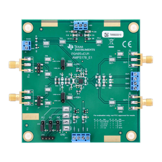
PGA855 Evaluation Module
This user's guide contains information and support documentation for the PGA855 evaluation module (EVM).
Included are the circuit description, jumper settings, required connections, printed circuit board (PCB) layout,
schematic, and bill of materials of the PGA855EVM. Throughout this document, the terms evaluation board,
evaluation module, and EVM are synonymous with the PGA855EVM.
SBOU296 – APRIL 2023
Submit Document Feedback
ABSTRACT
Copyright © 2023 Texas Instruments Incorporated
PGA855 Evaluation Module
1
Advertisement
Table of Contents

Subscribe to Our Youtube Channel
Related Manuals for Texas Instruments PGA855


Summary of Contents for Texas Instruments PGA855
- Page 1 PGA855 Evaluation Module ABSTRACT This user's guide contains information and support documentation for the PGA855 evaluation module (EVM). Included are the circuit description, jumper settings, required connections, printed circuit board (PCB) layout, schematic, and bill of materials of the PGA855EVM. Throughout this document, the terms evaluation board, evaluation module, and EVM are synonymous with the PGA855EVM.
-
Page 2: Table Of Contents
Table 5-1. PGA855EVM Analog Input and Output Connections....................8 Table 6-1. PGA855EVM Gain Control............................Table 8-1. PGA855EVM Bill of Materials........................... Trademarks All trademarks are the property of their respective owners. PGA855 Evaluation Module SBOU296 – APRIL 2023 Submit Document Feedback Copyright © 2023 Texas Instruments Incorporated... -
Page 3: Overview
(ADCs) and fully differential inputs. The PGA855 is equipped with eight binary gain settings, from an attenuating gain of 0.125 V/V to a maximum of 16 V/V, using three digital gain-selection pins. The output common-mode voltage can be independently set using the VOCM pin. -
Page 4: Evm Circuit Description
By default, the PGA855EVM programmable gain amplifier is configured to a gain of 0.125 V/V. The evaluation board provides shunt jumpers J10, J11, and J12 to set the PGA855 gain. The device uses two sets of voltage supplies: input stage and output stage. The output-stage power supplies are decoupled from the input stage to limit the PGA855 output-swing voltage level protecting the ADC or downstream device against overdrive damage. -
Page 5: Jumper Settings
Shunt 1-2: Sets A1 to VCC or 1 Open: Sets A0 to GND or 0 PGA gain CTRL A0 Open Shunt 1-2: Sets A0 to VCC or 1 SBOU296 – APRIL 2023 PGA855 Evaluation Module Submit Document Feedback Copyright © 2023 Texas Instruments Incorporated... -
Page 6: Power-Supply Connections
J14.4 Ground By default, the output-stage supply-voltage levels (+LVDD and –LVSS) are set to the PGA855 positive (+VCC) and negative (–VEE) supplies, respectively. The +LVDD pin is connected to +VCC through jumper J9 1-2, and the –LVSS pin is connected to –VEE through J16 1-2. Screw terminal connector J14 provides access to the output-stage supply pins. -
Page 7: Figure 4-1. Pga855Evm Voltage Supply Connections
100 nF LVDD+ 36 V VCC+ LVSS– VEE– TP16 100 nF 36 V 10 µF 100 nF LVSS– Figure 4-1. PGA855EVM Voltage Supply Connections SBOU296 – APRIL 2023 PGA855 Evaluation Module Submit Document Feedback Copyright © 2023 Texas Instruments Incorporated... -
Page 8: Analog Input And Output Connections
IN– OUT– OUT+ J4.4 OUT– Screw terminal J4.3 Screw terminal J4.2 Screw terminal J4.1 OUT+ Screw terminal J1.1 VOCM Screw terminal J1.2 Screw terminal PGA855 Evaluation Module SBOU296 – APRIL 2023 Submit Document Feedback Copyright © 2023 Texas Instruments Incorporated... -
Page 9: Digital Input Pins And Gain Control
The PGA855 provides eight binary gain settings, from an attenuating gain of 0.125 V/V to a maximum of 16 V/V. The gain is controlled by three digital selection pins: A0, A1, and A2. By default, the PGA855 is configured to a gain of 0.125 V/V. -
Page 10: Modifications
For flexibility, the EVM provides optional capacitors C4 and C18. These capacitors are in parallel with the PGA855 output-stage internal-feedback resistors to implement noise filtering. In addition, the evaluation board provides footprints R6, R10, C9, C5, and C12 for optional input low-pass filters, and footprints for load resistors R7 and R11. -
Page 11: Figure 8-2. Top Overlay Pcb Layout
Schematic, PCB Layout, and Bill of Materials Figure 8-2. Top Overlay PCB Layout SBOU296 – APRIL 2023 PGA855 Evaluation Module Submit Document Feedback Copyright © 2023 Texas Instruments Incorporated... -
Page 12: Figure 8-3. Top Layer Pcb Layout
Schematic, PCB Layout, and Bill of Materials www.ti.com Figure 8-3. Top Layer PCB Layout PGA855 Evaluation Module SBOU296 – APRIL 2023 Submit Document Feedback Copyright © 2023 Texas Instruments Incorporated... -
Page 13: Figure 8-4. Ground Layer Pcb Layout
Schematic, PCB Layout, and Bill of Materials Figure 8-4. Ground Layer PCB Layout SBOU296 – APRIL 2023 PGA855 Evaluation Module Submit Document Feedback Copyright © 2023 Texas Instruments Incorporated... -
Page 14: Figure 8-5. Power Layer Pcb Layout
Schematic, PCB Layout, and Bill of Materials www.ti.com Figure 8-5. Power Layer PCB Layout PGA855 Evaluation Module SBOU296 – APRIL 2023 Submit Document Feedback Copyright © 2023 Texas Instruments Incorporated... -
Page 15: Figure 8-6. Bottom Layer Pcb Layout
Schematic, PCB Layout, and Bill of Materials Figure 8-6. Bottom Layer PCB Layout SBOU296 – APRIL 2023 PGA855 Evaluation Module Submit Document Feedback Copyright © 2023 Texas Instruments Incorporated... -
Page 16: Bill Of Materials
R12, R13, R14, R15 RES, 0, 5%, 0.1 W, 0603 RC0603JR-070RL Yageo R16, R17, R18 10.0 kΩ RES, 10.0 k, 1%, 0.1 W, 0603 RCG060310K0FKEA Vishay Draloric PGA855 Evaluation Module SBOU296 – APRIL 2023 Submit Document Feedback Copyright © 2023 Texas Instruments Incorporated... - Page 17 TP16 TP12, TP13, TP14, Test Point, Compact, SMT Testpoint_Keystone_Comp 5016 Keystone TP17 Low-Noise, Wide-Bandwidth, Fully Differential VQFN17 PGA855RGT Texas Instruments Output, Programmable Gain Amplifier SBOU296 – APRIL 2023 PGA855 Evaluation Module Submit Document Feedback Copyright © 2023 Texas Instruments Incorporated...
- Page 18 STANDARD TERMS FOR EVALUATION MODULES Delivery: TI delivers TI evaluation boards, kits, or modules, including any accompanying demonstration software, components, and/or documentation which may be provided together or separately (collectively, an “EVM” or “EVMs”) to the User (“User”) in accordance with the terms set forth herein.
- Page 19 www.ti.com Regulatory Notices: 3.1 United States 3.1.1 Notice applicable to EVMs not FCC-Approved: FCC NOTICE: This kit is designed to allow product developers to evaluate electronic components, circuitry, or software associated with the kit to determine whether to incorporate such items in a finished product and software developers to write software applications for use with the end product.
- Page 20 www.ti.com Concernant les EVMs avec antennes détachables Conformément à la réglementation d'Industrie Canada, le présent émetteur radio peut fonctionner avec une antenne d'un type et d'un gain maximal (ou inférieur) approuvé pour l'émetteur par Industrie Canada. Dans le but de réduire les risques de brouillage radioélectrique à...
- Page 21 www.ti.com EVM Use Restrictions and Warnings: 4.1 EVMS ARE NOT FOR USE IN FUNCTIONAL SAFETY AND/OR SAFETY CRITICAL EVALUATIONS, INCLUDING BUT NOT LIMITED TO EVALUATIONS OF LIFE SUPPORT APPLICATIONS. 4.2 User must read and apply the user guide and other available documentation provided by TI regarding the EVM prior to handling or using the EVM, including without limitation any warning or restriction notices.
- Page 22 Notwithstanding the foregoing, any judgment may be enforced in any United States or foreign court, and TI may seek injunctive relief in any United States or foreign court. Mailing Address: Texas Instruments, Post Office Box 655303, Dallas, Texas 75265 Copyright © 2023, Texas Instruments Incorporated...
- Page 23 TI products. TI’s provision of these resources does not expand or otherwise alter TI’s applicable warranties or warranty disclaimers for TI products. TI objects to and rejects any additional or different terms you may have proposed. IMPORTANT NOTICE Mailing Address: Texas Instruments, Post Office Box 655303, Dallas, Texas 75265 Copyright © 2023, Texas Instruments Incorporated...
Need help?
Do you have a question about the PGA855 and is the answer not in the manual?
Questions and answers