
Related Manuals for Quectel EG25-GL


Summary of Contents for Quectel EG25-GL
- Page 1 EG25-GL Hardware Design LTE Standard Module Series Version: 1.0.0 Date: 2022-09-09 Status: Preliminary...
- Page 2 LTE Standard Module Series At Quectel, our aim is to provide timely and comprehensive services to our customers. If you require any assistance, please contact our headquarters: Quectel Wireless Solutions Co., Ltd. Building 5, Shanghai Business Park Phase III (Area B), No.1016 Tianlin Road, Minhang District, Shanghai...
- Page 3 Except as otherwise set forth herein, nothing in this document shall be construed as conferring any rights to use any trademark, trade name or name, abbreviation, or counterfeit product thereof owned by Quectel or any third party in advertising, publicity, or other aspects.
-
Page 4: Safety Information
Manufacturers of the cellular terminal should notify users and operating personnel of the following safety information by incorporating these guidelines into all manuals of the product. Otherwise, Quectel assumes no liability for your failure to comply with these precautions. -
Page 5: About The Document
LTE Standard Module Series About the Document Revision History Version Date Author Description 2022-09-09 Ethan FANG/Joe MA Creation of the document 1.0.0 2022-09-09 Ethan FANG/Joe MA Preliminary EG25-GL_Hardware_Design 4 / 96... -
Page 6: Table Of Contents
LTE Standard Module Series Contents Safety Information ............................3 About the Document ........................... 4 Contents ............................... 5 Table Index ..............................8 Figure Index ............................... 10 Introduction ............................12 Special Marks .......................... 12 Product Overview ..........................13 Frequency Bands and Functions ..................... 13 Key Features ........................... - Page 7 LTE Standard Module Series SD Card Interface ........................48 WLAN and Bluetooth Application Interfaces ................50 4.6.1 WLAN Application Interface ................... 53 4.6.2 Bluetooth Application Interface* ..................53 ADC Interfaces ........................53 SGMII Interface ........................54 Indication Signals........................56 4.9.1 Network Status Indication ....................
- Page 8 LTE Standard Module Series Appendix References ........................92 EG25-GL_Hardware_Design 7 / 96...
- Page 9 Table Index Table 1: Special Marks ..........................12 Table 2: Frequency Bands and Functions ....................13 Table 3: Key Features of EG25-GL Module ....................14 Table 4: I/O Parameters Definition ......................19 Table 5: Pin Description ..........................20 Table 6: Overview of Operating Modes ...................... 28 Table 7: Pin Definition of VBAT and GND Pins ..................
- Page 10 LTE Standard Module Series Table 42: Terms and Abbreviations ......................92 EG25-GL_Hardware_Design 9 / 96...
- Page 11 LTE Standard Module Series Figure Index Figure 1: Functional Diagram ........................17 Figure 2: Pin Assignment (Top View) ......................18 Figure 3: Sleep Mode Application via UART ....................29 Figure 4: Sleep Mode Application with USB Remote Wakeup ..............30 Figure 5: Sleep Mode Application with MAIN_RI ..................
- Page 12 LTE Standard Module Series Figure 42: Module Top and Side Dimensions .................... 81 Figure 43: Bottom Dimensions (Bottom View) ................... 82 Figure 44: Recommended Footprint (Top View) ..................83 Figure 45: Recommended Compatible Footprint (Top View) ..............84 Figure 46: Top and Bottom Views of the Module ..................85 Figure 47: Recommended Reflow Soldering Thermal Profile ..............
-
Page 13: Introduction
LTE Standard Module Series Introduction This document defines EG25-GL module and describes its air interface and hardware interfaces which are connected with your applications. With this document, you can quickly understand module interface specifications, electrical and mechanical details, as well as other related information of the module. The document, coupled with application notes and user guides, makes it easy to design and set up mobile applications with the module. -
Page 14: Product Overview
VoLTE (Voice over LTE) Optional With a compact profile of 29.0 mm × 32.0 mm × 2.4 mm, EG25-GL can meet most requirements for M2M applications such as automation, smart metering, tracking system, security, router, wireless POS, mobile computing device, PDA phone, tablet PC, etc. -
Page 15: Key Features
LTE Standard Module Series 2.2 Key Features The following table describes the detailed features of EG25-GL module. Table 3: Key Features of EG25-GL Module Features Description ⚫ Supply voltage: 3.3–4.3 V Power Supply ⚫ Typical supply voltage: 3.8 V ⚫... - Page 16 ⚫ Data update rate: 1 Hz by default ⚫ Compliant with 3GPP TS 27.007, 3GPP TS 27.005 AT Commands ⚫ Compliant with Quectel enhanced AT commands ⚫ Two pins NET_MODE and NET_STATUS to indicate network connectivity Network Indication status EG25-GL_Hardware_Design...
- Page 17 LTE Standard Module Series ⚫ Main antenna interface (ANT_MAIN) ⚫ Antenna Interfaces Rx-diversity antenna interface (ANT_DIV) ⚫ GNSS antenna interface (ANT_GNSS) ⚫ Size: (29.0 ± 0.2) mm × (32.0 ± 0.2) mm × (2.4 ± 0.2) mm Physical ⚫ Package: LGA Characteristics ⚫...
-
Page 18: Functional Diagram
LTE Standard Module Series 2.3 Functional Diagram The following figure shows a block diagram of EG25-GL and illustrates the major functional parts. ⚫ Power management ⚫ Baseband ⚫ DDR2+NAND flash ⚫ Radio frequency ⚫ Peripheral interfaces ANT_MAIN ANT_GNSS ANT_DIV Switch... -
Page 19: Pin Assignment
LTE Standard Module Series 2.4 Pin Assignment The following figure shows the pin assignment of EG25-GL module. WAKEUP_IN AP_READY RESERVED W_DISABLE# NET_MODE NET_ST ATUS ANT_MAIN VDD_EXT RESERVED RESERVED RESERVED RESERVED ANT_GNSS USIM_GND ADC0 DBG_RXD ADC1 DBG_TXD RESERVED USIM_DET I2C_SDA USIM_VDD... -
Page 20: Pin Description
118, 127 and 129–138 are WLAN function pins, and the rest are Bluetooth function* pins. Pins 119–126 and 128 are used for SGMII interface. Pins 24–27 of PCM interface can be used not only for audio function on EG25-GL module, but also for Bluetooth function* on FC20 series or FC21 module. - Page 21 LTE Standard Module Series Table 5: Pin Description Power Supply Pin Name Pin No. Description DC Characteristics Comment It must be provided Power supply for the VBAT_BB 59, 60 with sufficient current module’s BB part up to 0.8 A. Vmax = 4.3 V Vmin = 3.3 V It must be provided Vnom = 3.8 V...
- Page 22 LTE Standard Module Series 1.8 V power domain. Indicate the module’s NET_STATUS VDD_EXT If unused, keep it network activity status open. USB Interface Pin Name Pin No. Description DC Characteristics Comment Vmax = 5.25 V Typical: 5.0 V USB connection USB_VBUS Vmin = 3.0 V If unused, keep it...
- Page 23 LTE Standard Module Series Main UART data open. MAIN_DCD VDD_EXT carrier detect Connect to DTE’s CTS. DTE clear to send MAIN_CTS VDD_EXT 1.8 V power domain. signal from DCE If unused, keep it open. Connect to DTE's RTS. DTE request to send MAIN_RTS VDD_EXT 1.8 V power domain.
- Page 24 SD 3.0 protocol for more details. If unused, keep it open. Pins (Pin 24–27) of PCM interface can be used not only for audio function on EG25-GL module, but also for Bluetooth function* on FC20 series or FC21 module. EG25-GL_Hardware_Design...
- Page 25 LTE Standard Module Series SDIO signal level can be selected according to SD card supported level, see SD_CMD SD card command SD_PU_VDD SD 3.0 protocol for more details. If unused, keep it open. 1.8 V power domain. SD card insertion SD_DET VDD_EXT If unused, keep it...
- Page 26 LTE Standard Module Series 1.8 V power domain. Active high. WLAN function Cannot be pulled up WLAN_EN VDD_EXT enable control before startup. If unused, keep it open. LTE & WLAN/ 1.8 V power domain. COEX_RXD Bluetooth coexistence VDD_EXT Cannot be pulled up receive before startup.
- Page 27 LTE Standard Module Series Require external pull-up to SGMII_MDIO_VDD, and the resistor should be 1.5 kΩ. If unused, keep it open. 1.8/2.85 V power SGMII management domain. SGMII_MDC SGMII_MDIO_VDD data clock If unused, keep it open. Connect with a SGMII_TX_M SGMII transmit (-) 0.1 μF capacitor, which is close to the...
-
Page 28: Evb Kit
3, 18, 43, 55, 73–84, 113, 114, 116, 117, 140–144 unconnected. 2.6 EVB Kit To help you develop applications with the module, Quectel supplies an evaluation board (UMTS<E EVB) with accessories to control or test the module. For more details, see document [1]. EG25-GL_Hardware_Design... -
Page 29: Operating Characteristics
LTE Standard Module Series Operating Characteristics 3.1 Operating Modes The following table briefly outlines the operating modes to be mentioned in the following chapters. Table 6: Overview of Operating Modes Mode Details Software is active. The module has registered on the network, and it is Idle ready to send and receive data. -
Page 30: Sleep Mode
LTE Standard Module Series 3.2 Sleep Mode 3.2.1 UART Application Scenario If the host communicates with module via UART interfaces, the following preconditions can let the module enter sleep mode. ⚫ Execute AT+QSCLK=1 to enable sleep mode. For details of the command, see document [2]. ⚫... -
Page 31: Usb Application With Usb Suspend/Resume And Main_Ri Function
LTE Standard Module Series The following figure shows the connection between the module and the host. Host Module USB_VBUS USB_DP USB_DP USB_DM USB_DM GPIO AP_READY Figure 4: Sleep Mode Application with USB Remote Wakeup ⚫ Sending data to the module through USB will wake up the module. ⚫... -
Page 32: Usb Application Without Usb Suspend Function
LTE Standard Module Series ⚫ Sending data to the module via USB will wake up the module. ⚫ When the module has a URC to report, MAIN_RI signal will wake up the host. 3.2.2.3 USB Application without USB Suspend Function If the host does not support USB suspend function, USB_VBUS should be disconnected with an external control circuit to set the module to sleep mode. -
Page 33: Power Supply
LTE Standard Module Series Hardware: The W_DISABLE# pin is pulled up by default. Driving it to low level will let the module enter airplane mode. Software: AT+CFUN provides the choice of the functionality level through setting <fun> into 0, 1 or 4. ⚫... -
Page 34: Voltage Stability Requirements
LTE Standard Module Series 3.3.2 Voltage Stability Requirements The power supply range of the module is from 3.3 V to 4.3 V. Please make sure that the input voltage will never drop below 3.3 V. The following figure shows the voltage drop during burst transmission in 2G network. -
Page 35: Reference Design For Power Supply
LTE Standard Module Series VBAT VBAT_RF VBAT_BB 100 μF 4.5 V 100 μF 100 nF 33 pF 100 pF 100 nF 33 pF 10 pF Module Figure 8: Star Structure of the Power Supply 3.3.3 Reference Design for Power Supply Power design for the module is very important, as the performance of the module largely depends on the power source. -
Page 36: Power Supply Voltage Monitoring
LTE Standard Module Series NOTE To avoid corrupting the data in the internal flash, do not switch off the power supply when the module works normally. Only after shutting down the module with PWRKEY or AT command can you cut off the power supply. - Page 37 LTE Standard Module Series The other way to control the PWRKEY is using a button directly. When pressing the button, electrostatic strike may generate from finger. Therefore, a TVS component is indispensable to be placed nearby the button for ESD protection. A reference circuit is shown in the following figure. PWRKEY Close to S1 Figure 11: Turn On the Module by Using a Button...
-
Page 38: Turn Off
LTE Standard Module Series NOTE 1. Make sure that VBAT is stable before pulling down PWRKEY pin. It is recommended that the time between powering up VBAT and pulling down PWRKEY pin is not less than 30 ms. 2. PWRKEY can be pulled down directly to GND with a recommended 10 kΩ resistor if the module needs to be turned on automatically and shutdown is not needed. -
Page 39: Reset
LTE Standard Module Series NOTE 1. To avoid corrupting the data in the internal flash, do not switch off the power supply when the module works normally. Only after turning off the module with PWRKEY or AT command can you cut off the power supply. - Page 40 LTE Standard Module Series RESET_N Close to S2 Figure 15: Reference Circuit of RESET_N by Using a Button The reset scenario is illustrated in the following figure. VBAT 460 ms 150 ms 1.3 V RESET_N 0.5 V Module Running Resetting Restart Status Figure 16: Reset Timing...
-
Page 41: Application Interfaces
LTE Standard Module Series Application Interfaces 4.1 (U)SIM Interface The (U)SIM interface circuitry meets ETSI and IMT-2000 requirements. Either 1.8 V or 3.0 V (U)SIM card is supported. Table 10: Pin Definition of (U)SIM Interface Pin Name Description Comment Either 1.8 V or 3.0 V is supported USIM_VDD (U)SIM card power supply by the module automatically. - Page 42 LTE Standard Module Series VDD_EXT USIM_VDD 100 nF (U)SIM Card Connector USIM_GND USIM_VDD USIM_RST Module USIM_CLK USIM_DET USIM_DATA 33 pF 33 pF 33 pF TVS array Figure 17: Reference Circuit of (U)SIM Interface with an 8-pin (U)SIM Card Connector If (U)SIM card detection function is not needed, keep USIM_DET unconnected. A reference circuit of (U)SIM interface with a 6-pin (U)SIM card connector is illustrated in the following figure.
-
Page 43: Usb Interface
LTE Standard Module Series be connected to PCB ground directly. ⚫ To avoid cross-talk between USIM_DATA and USIM_CLK, keep them away from each other and shield them with surrounded ground. ⚫ In order to offer good ESD protection, it is recommended to add a TVS array whose parasitic capacitance should not be more than 15 pF. -
Page 44: Uart Interfaces
LTE Standard Module Series Test Points Minimize these stubs Module NM_0R NM_0R ESD Array USB_VBUS USB_DM USB_DM USB_DP USB_DP Close to Module Figure 19: Reference Circuit of USB Interface A common-mode choke L1 is recommended to be added in series between the module and your MCU to suppress EMI spurious transmission. - Page 45 LTE Standard Module Series 921600 bps baud rates, and the default is 115200 bps. It also supports RTS and CTS hardware flow control, and can be used for data transmission and AT command communication. ⚫ The debug UART interface supports 115200 bps baud rate. It is used for Linux console and log output.
- Page 46 LTE Standard Module Series VDD_EXT VCCA VCCB VDD_MCU 0.1 μF 0.1 μF 120K MAIN_RI RI_MCU MAIN_DCD DCD_MCU Translator MAIN_CTS CTS_MCU MAIN_RTS RTS_MCU MAIN_DTR DTR_MCU MAIN_TXD TXD_MCU MAIN_RXD RXD_MCU Figure 20: Reference Circuit with Translator Chip Visit http://www.ti.com for more information. Another example with transistor translation circuit is shown as below.
-
Page 47: Pcm And I2C Interfaces
LTE Standard Module Series 4.4 PCM and I2C Interfaces The module provides one Pulse Code Modulation (PCM) digital interface for audio design, which supports the following modes, and one I2C interface: ⚫ Primary mode (short frame synchronization, works as both master and slave) ⚫... - Page 48 LTE Standard Module Series 125 μs PCM_CLK PCM_SYNC PCM_DOUT PCM_DIN Figure 23: Auxiliary Mode Timing The following table shows the pin definition of PCM and I2C interfaces which can be applied on audio codec design. Table 14: Pin Definition of PCM and I2C Interfaces Pin Name Pin No.
-
Page 49: Sd Card Interface
LTE Standard Module Series MICBIAS PCM_CLK BCLK PCM_SYNC LRCK PCM_DOUT PCM_DIN LOUTP I2C_SCL I2C_SDA LOUTN Module Codec 1.8 V Figure 24: Reference Circuit of PCM and I2C Application with Audio Codec NOTE It is recommended to reserve an RC (R = 22 Ω, C = 22 pF) circuits on the PCM lines, especially for PCM_CLK. - Page 50 LTE Standard Module Series SDIO signal level can be selected according to SD card supported level, see SD_CMD SD card command SD 3.0 protocol for more details. If unused, keep it open. SD card insertion 1.8 V power domain. SD_DET detect If unused, keep it open.
-
Page 51: Wlan And Bluetooth Application Interfaces
LTE Standard Module Series ⚫ It is important to route the SDIO signal traces with total grounding. The impedance of SDIO data trace is 50 Ω (± 10%). ⚫ Make sure the adjacent trace spacing is twice of the trace width and the load capacitance of SDIO bus should be less than 15 pF. - Page 52 The following figure shows a reference design of WLAN and Bluetooth application interfaces with Quectel FC20 series or FC21 module. Pins (Pin 24–27) of PCM interface can be used not only for audio function on EG25-GL module, but also for Bluetooth function* on FC20 series or FC21 module.
- Page 53 LTE Standard Module Series FC20 Series/ FC21 Module Module WLAN_PWR_EN DC-DC/LDO VDD_3V3 POWER VDD_EXT SDC_DATA3 SDIO_D3 SDC_DATA2 SDIO_D2 SDC_DATA1 SDIO_D1 SDC_DATA0 SDIO_D0 WLAN SDC_CLK SDIO_CLK SDC_CMD SDIO_CMD WLAN_EN WLAN_EN WLAN_SLP_CLK 32KHz_IN WAKE_ON_WIREL ESS WAKE_ON_WIREL ESS COEX_RXD LTE_UART_TXD COEX COEX_TXD LTE_UART_RXD BT_EN BT_EN BT_RTS...
-
Page 54: Wlan Application Interface
LTE Standard Module Series 4.6.1 WLAN Application Interface The module provides a SDIO 3.0 interface and control interface for WLAN design. SDIO interface supports SDR mode, and the maximum frequency is up to 50 MHz. As SDIO signals are very high-speed, in order to ensure the SDIO interface design corresponds with the SDIO 3.0 specification, please comply with the following principles: ⚫... -
Page 55: Sgmii Interface
LTE Standard Module Series The following table describes the characteristic of ADC function. Table 18: Characteristic of ADC Parameter Min. Typ. Max. Unit ADC0 Voltage Range VBAT_BB ADC1 Voltage Range VBAT_BB ADC Resolution bits NOTE ADC input voltage must not exceed that of VBAT_BB. It is prohibited to supply any voltage to ADC pins when VBAT power supply is removed. - Page 56 LTE Standard Module Series 1.8 V power domain. SGMII_INT_N Ethernet PHY interrupt If unused, keep it open. 1.8/2.85 V power domain. Require external pull-up to SGMII_MDIO DIO SGMII management data SGMII_MDIO_VDD, and the resistor should be 1.5 kΩ. If unused, keep it open. SGMII management data 1.8/2.85 V power domain.
-
Page 57: Indication Signals
LTE Standard Module Series Module AR8033 VDD_EXT 1.5K SGMII_MDIO_VDD SGMII_INT_N SGMII_RST_N RSTN Control SGMII_MDIO MDIO SGMII_MDC SGMII_MDIO_VDD SGMII_MDIO_VDD Close to Module 0.1 μF SGMII_RX_P 0.1 μF SGMII_RX_M SGMII Data 0.1 μF SGMII_TX_P 0.1 μF SGMII_TX_M Close to AR8033 Figure 28: Reference Circuit of SGMII Interface with PHY AR8033 Application In order to enhance the reliability and availability in your applications, please follow the criteria below in the Ethernet PHY circuit design: ⚫... - Page 58 LTE Standard Module Series Table 20: Pin Definition of Network Connection Status/Activity Indication Pin Name Pin No. Description Comment 1.8 V power domain. Cannot be Indicate the module’s network NET_MODE pulled up before startup. registration mode If unused, keep it open. Indicate the module’s network 1.8 V power domain.
-
Page 59: Status
LTE Standard Module Series 4.9.2 STATUS The STATUS pin is an open drain output for indicating the module’s operation status. It can be connected to a GPIO of DTE with a pull-up resistor, or as LED indication circuit as below. When the module is turned on normally, the STATUS will present the low state. -
Page 60: Usb_Boot
LTE Standard Module Series Table 23: Behaviors of MAIN_RI State Response Idle MAIN_RI keeps at high level MAIN_RI outputs 120 ms low pulse when a new URC returns NOTE A URC can be outputted from UART port, USB AT port and USB modem port through configuration via AT+QURCCFG. - Page 61 LTE Standard Module Series Module VDD_EXT Test points 4.7K USB_BOOT Close to test points Figure 31: Reference Circuit of USB_BOOT Interface NOTE 1 VBAT 500 ms PWRKEY 0.5 V About 100 ms USB_BOOT can be pulled up to 1.8 V before VDD_EXT VDD_EXT Is powered up, and the module will enter emergency download mode when it is...
-
Page 62: Rf Specifications
LTE Standard Module Series RF Specifications 5.1 Cellular Network 5.1.1 Antenna Interface & Frequency Bands The pin definition of main antenna and Rx-diversity antenna interfaces is shown below. Table 25: Pin Definition of Antenna Antennas Pin Name Pin No. Description Comment 50 Ω... - Page 63 LTE Standard Module Series WCDMA B8 880–915 925–960 WCDMA B19 830–845 875–890 LTE-FDD B1 1920–1980 2110–2170 LTE-FDD B2 1850–1910 1930–1990 LTE-FDD B3 1710–1785 1805–1880 LTE-FDD B4 1710–1755 2110–2155 LTE-FDD B5 824–849 869–894 LTE-FDD B7 2500–2570 2620–2690 LTE-FDD B8 880–915 925–960 LTE-FDD B12 699–716 729–746...
-
Page 64: Tx Power
GSM specification as described in Chapter 13.16 of 3GPP TS 51.010-1. 5.1.3 Rx Sensitivity The following tables show the conducted RF receiving sensitivity of the module. Table 28: EG25-GL Conducted RF Receiving Sensitivity Receiving Sensitivity (Typ.) Frequency Bands 3GPP (SIMO) - Page 65 LTE Standard Module Series DCS1800 -107 dBm -102.4 dBm PCS1900 -107.5 dBm -102.4 dBm WCDMA B1 -108dBm -109 dBm -110 dBm -106.7 dBm WCDMA B2 -108 dBm -108 dBm -110 dBm -104.7 dBm WCDMA B4 -107 dBm -109 dBm -109 dBm -106.7 dBm WCDMA B5 -109.5 dBm...
-
Page 66: Reference Design
LTE Standard Module Series LTE-TDD B38 (10 MHz) -97 dBm -97 dBm -100 dBm -96.3 dBm LTE-TDD B39 (10 MHz) -97.5 dBm -97.5 dBm -100 dBm -96.3 dBm LTE-TDD B40 (10 MHz) -97.3 dBm -97.5 dBm -100.5dBm -96.3 dBm LTE-TDD B41 (10 MHz) -96.3 dBm -97 dBm -99.5 dBm... -
Page 67: Gnss
LTE Standard Module Series 5.2 GNSS 5.2.1 Antenna Interface & Frequency Bands The module includes a fully integrated global navigation satellite system solution that supports GPS, GLONASS, BDS, Galileo and QZSS. The module supports standard NMEA 0183 protocol, and outputs NMEA sentences at 1 Hz data update rate via USB interface by default. -
Page 68: Gnss Performance
LTE Standard Module Series 0.1 μF GNSS Antenna Module 47 nH 100 pF ANT_GNSS Figure 34: Reference Circuit of GNSS Antenna NOTE An external LDO can be selected to supply power according to the active antenna requirement. If the module is designed with a passive antenna, then the VDD circuit is not needed. It is recommended to use a passive GNSS antenna when LTE B13 is supported, as the use of active antenna may generate harmonics which will affect the GNSS performance. -
Page 69: Reference Design
LTE Standard Module Series Autonomous Hot start @ open sky XTRA enabled Autonomous Accuracy CEP-50 @ open sky NOTE Tracking sensitivity: the minimum GNSS signal power at which the module can maintain lock (keep positioning for at least 3 minutes continuously). Reacquisition sensitivity: the minimum GNSS signal power required for the module to maintain lock within 3 minutes after loss of lock. - Page 70 LTE Standard Module Series Figure 35: Microstrip Design on a 2-layer PCB Figure 36: Coplanar Waveguide Design on a 2-layer PCB Figure 37: Coplanar Waveguide Design on a 4-layer PCB (Layer 3 as Reference Ground) EG25-GL_Hardware_Design 69 / 96...
-
Page 71: Antenna Design Requirements
LTE Standard Module Series Figure 38: Coplanar Waveguide Design on a 4-layer PCB (Layer 4 as Reference Ground) To ensure RF performance and reliability, follow the principles below in RF layout design: ⚫ Use an impedance simulation tool to accurately control the characteristic impedance of RF traces to 50 Ω. -
Page 72: Rf Connector Recommendation
LTE Standard Module Series ⚫ Passive antenna gain: > 0 dBi ⚫ Active antenna noise figure: < 1.5 dB ⚫ Active antenna gain: > 0 dBi ⚫ Active antenna embedded LNA gain: < 17 dB ⚫ VSWR: ≤ 2 ⚫ Efficiency: >... - Page 73 LTE Standard Module Series Figure 40: Specifications of Mated Plugs The following figure describes the space factor of mated connectors. Figure 41: Space Factor of Mated Connectors (Unit: mm) For more details, visit http://www.hirose.com EG25-GL_Hardware_Design 72 / 96...
-
Page 74: Electrical Characteristics And Reliability
LTE Standard Module Series Electrical Characteristics and Reliability 6.1 Absolute Maximum Ratings Absolute maximum ratings for power supply and voltage on digital and analog pins of the module are listed in the following table. Table 33: Absolute Maximum Ratings Parameter Min. -
Page 75: Power Supply Ratings
Maximum power control (during transmission VBAT level on EGSM900. slot) USB connection USB_VBUS 5.25 detection 6.3 Power Consumption Table 35: EG25-GL Current Consumption Description Conditions Typ. Unit μA Power-off Power down AT+CFUN=0 (USB disconnected) AT+CFUN=0 (USB suspended) AT+CFUN=4 (USB disconnected) - Page 76 LTE Standard Module Series DCS1800 @ DRX = 2 (USB disconnected) DCS1800 @ DRX = 5 (USB disconnected) DCS1800 @ DRX = 5 (USB suspended) DCS1800 @ DRX = 9 (USB disconnected) WCDMA @ PF = 64 (USB disconnected) WCDMA @ PF = 64 (USB suspended) WCDMA @ PF = 128 (USB disconnected) WCDMA @ PF = 256 (USB disconnected) WCDMA @ PF = 512 (USB disconnected)
- Page 77 LTE Standard Module Series LTE-TDD @ PF = 64 (USB disconnected) 16.4 LTE-TDD @ PF = 64 (USB connected) 26.2 EGSM900 4DL/1UL @ 32 dBm EGSM900 3DL/2UL @ 31.09dBm EGSM900 2DL/3UL @ 29.2 dBm EGSM900 1DL/4UL @ 28.1 dBm GSM850 4DL/1UL @ 31.97 dBm GSM850 3DL/2UL @ 30.08 dBm GSM850 2DL/3UL @ 29.08 dBm GPRS Data...
- Page 78 LTE Standard Module Series GSM850 1DL/4UL @ 21.71 dBm DCS1800 4DL/1UL @ 25.19 dBm DCS1800 3DL/2UL @ 24.61 dBm DCS1800 2DL/3UL @ 23.48 dBm DCS1800 1DL/4UL @ 22.25 dBm PCS1900 4DL/1UL @ 25.24 dBm PCS1900 3DL/2UL @ 24.76 dBm PCS1900 2DL/3UL @ 23.6 dBm PCS1900 1DL/4UL @ 22.27 dBm WCDMA B1 HSDPA @ 22.6 dBm WCDMA B1 HSUPA @ 22.4 dBm...
- Page 79 LTE Standard Module Series LTE-FDD B3 @ 23.52 dBm LTE-FDD B4 @ 23.42 dBm LTE-FDD B5 @ 23.27 dBm LTE-FDD B7 @ 23.3 dBm 1050 LTE-FDD B8 @ 23.14 dBm LTE-FDD B12 @ 23.33 dBm LTE-FDD B13 @ 23.2 dBm LTE-FDD B18 @ 23.2 dBm LTE-FDD B19 @ 23.02 dBm LTE-FDD B20 @ 23.16 dBm...
-
Page 80: Esd Protection
LTE Standard Module Series DCS1800 PCL = 0 @ 28.91 dBm DCS1800 PCL = 7 @ 15.83 dBm DCS1800 PCL = 15 @ -2.91 dBm PCS1900 PCL = 0 @ 29.31 dBm 170- PCS1900 PCL = 7 @ 15.81 dBm PCS1900 PCL = 15 @ -2.75 dBm WCDMA B1 @ 23.65 dBm WCDMA B2 @ 23.96 dBm... -
Page 81: Operating And Storage Temperatures
LTE Standard Module Series 6.5 Operating and Storage Temperatures The operating and storage temperatures are listed in the following table. Table 37: Operating and Storage Temperatures Parameter Min. Typ. Max. Unit Operating Temperature Range º C Extended Temperature Range º C Storage Temperature Range º... -
Page 82: Mechanical Information
LTE Standard Module Series Mechanical Information This chapter describes the mechanical dimensions of the module. All dimensions are measured in mm, and the dimensional tolerances are ± 0.2 mm unless otherwise specified. 7.1 Mechanical Dimensions Figure 42: Module Top and Side Dimensions EG25-GL_Hardware_Design 81 / 96... - Page 83 LTE Standard Module Series Figure 43: Bottom Dimensions (Bottom View) NOTE The package warpage level of the module conforms to the JEITA ED-7306 standard. EG25-GL_Hardware_Design 82 / 96...
-
Page 84: Recommended Footprint
LTE Standard Module Series 7.2 Recommended Footprint Figure 44: Recommended Footprint (Top View) NOTE The keepout area should not be designed. Keep at least 3 mm between the module and other components on the motherboard to improve soldering quality and maintenance convenience. EG25-GL_Hardware_Design 83 / 96... -
Page 85: Recommended Compatible Footprint
PCB. LGA form factor is used for EG25-GL module, while LCC is recommended only in the compatible design with EC25 series/EC21 series/EC20-CE/EG21-G/EG25-G/EC200A series modules. If you use LCC form factor, you should choose the stencil matched with LGA package instead of that matched with LCC package. -
Page 86: Top And Bottom Views
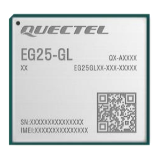
Figure 46: Top and Bottom Views of the Module NOTE Images above are for illustration purpose only and may differ from the actual module. For authentic appearance and label, please refer to the module received from Quectel. EG25-GL_Hardware_Design 85 / 96... -
Page 87: Storage, Manufacturing And Packaging
LTE Standard Module Series Storage, Manufacturing and Packaging 8.1 Storage Conditions The module is provided with vacuum-sealed packaging. MSL of the module is rated as 3. The storage requirements are shown below. 1. Recommended Storage Condition: the temperature should be 23 ± 5 ° C and the relative humidity should be 35–60 %. -
Page 88: Manufacturing And Soldering
LTE Standard Module Series NOTE 1. To avoid blistering, layer separation and other soldering issues, extended exposure of the module to the air is forbidden. 2. Take out the module from the package and put it on high-temperature-resistant fixtures before baking. If shorter baking time is desired, see IPC/JEDEC J-STD-033 for the baking procedure. -
Page 89: Packaging Specifications
2. Avoid using ultrasonic technology for module cleaning since it can damage crystals inside the module. 3. Due to the complexity of the SMT process, please contact Quectel Technical Support in advance for any situation that you are not sure about, or any process (e.g. selective soldering, ultrasonic soldering) that is not mentioned in document [8]. -
Page 90: Carrier Tape
LTE Standard Module Series 8.3.1 Carrier Tape Dimension details are as follow: Figure 48: Carrier Tape Dimension Drawing Table 39: Carrier Tape Dimension Table (Unit: mm) 0.35 32.5 29.5 20.2 1.75 8.3.2 Plastic Reel Figure 49: Plastic Reel Dimension Drawing EG25-GL_Hardware_Design 89 / 96... -
Page 91: Packaging Process
LTE Standard Module Series Table 40: Plastic Reel Dimension Table (Unit: mm) øD1 øD2 44.5 8.3.3 Packaging Process Place the module into the carrier tape and use the cover tape to cover it; then wind the heat-sealed carrier tape to the plastic reel and use the protective tape for protection. - Page 92 LTE Standard Module Series Put 4 packaged pizza boxes into 1 carton box and seal it. 1 carton box can pack 1000 modules. Figure 50: Packaging Process EG25-GL_Hardware_Design 91 / 96...
- Page 93 LTE Standard Module Series 9. Appendix References Table 41: Related Documents Document Name [1] Quectel_UMTS<E_EVB_User_Guide [2] Quectel_EC2x&EG2x-G(L)&EG9x&EM05_Series_AT_Commands_Manual [3] Quectel_EC2x&EG2x-G(L)&EG9x&EM05_Series_QCFG_AT_Commands_Manual [4] Quectel_EC2x&EG9x&EG2x-G(L)_Series_Power_Management_Application_Note [5] Quectel_EG25-GL_Reference_Design [6] Quectel_EC2x&EG2x-G(L)&EG9x&EM05_Series_GNSS_Application_Note [7] Quectel_RF_Layout_Application_Note [8] Quectel_Module_Secondary_SMT_Application_Note Table 42: Terms and Abbreviations Abbreviation Description Adaptive Multi-rate AMR-WB Adaptive Multi-Rate Wideband Bits Per Second CHAP Challenge Handshake Authentication Protocol...
- Page 94 LTE Standard Module Series Double Data Rate DFOTA Delta Firmware Upgrade Over The Air Downlink Data Terminal Ready Discontinuous Transmission EDGE Enhanced Data Rates for GSM Evolution Enhanced Full Rate EGSM Enhanced GSM Electrostatic Discharge Evaluation Board Frequency Division Duplex Full Rate File Transfer Protocol FTPS...
- Page 95 LTE Standard Module Series Input/Output Light Emitting Diode Land Grid Array Low Noise Amplifier Long Term Evolution Machine to Machine Modulation and Coding Scheme Mobile Equipment MIMO Multiple Input Multiple Output Multimedia Messaging Service Mobile Originated MQTT Message Queuing Telemetry Transport Mobile Station (GSM engine) Moisture Sensitivity Level Mobile Terminated...
- Page 96 LTE Standard Module Series Point-to-Point Protocol Quadrature Amplitude Modulation QPSK Quadrature Phase Shift Keying QZSS Quasi-Zenith Satellite System Radio Frequency RHCP Right Hand Circularly Polarized Ready To Send Receive Software-Defined Radio SGMII Serial Gigabit Media Independent Interface SIMO Single Input Multiple Output Surface Mount Device Short Message Service SMTP...
- Page 97 LTE Standard Module Series VLAN Virtual Local Area Network Vmax Maximum Voltage Vnom Normal Voltage Vmin Minimum Voltage Maximum High-level Input Voltage Minimum High-level Input Voltage Maximum Low-level Input Voltage Minimum Low-level Input Voltage Maximum High-level Output Voltage Minimum High-level Output Voltage Maximum Low-level Output Voltage Minimum Low-level Output Voltage VSWR...
- Page 98 Quectel that they wish to change the antenna trace design. In this case, a Class II permissive change application is required to be filed by...
- Page 99 Antenna (1) The antenna must be installed such that 20 cm is maintained between the antenna and users, (2) The transmitter module may not be co-located with any other transmitter or antenna. In the event that these conditions cannot be met (for example certain laptop configurations or co-location with another transmitter), then the FCC/IC authorization is no longer considered valid and the FCC ID/IC ID cannot be used on the final product.
- Page 100 Manual Information to the End User The OEM integrator has to be aware not to provide information to the end user regarding how to install or remove this RF module in the user’s manual of the end product which integrates this module. The end user manual shall include all required regulatory information/warning as show in this manual...
- Page 101 Federal Communication Commission Interference Statement This device complies with Part 15 of the FCC Rules. Operation is subject to the following two conditions: (1) This device may not cause harmful interference, and (2) this device must accept any interference received, including interference that may cause undesired operation. This equipment has been tested and found to comply with the limits for a Class B digital device, pursuant to Part 15 of the FCC Rules.
- Page 102 This device is intended only for OEM integrators under the following conditions: (For module device use) 1) The antenna must be installed such that 20 cm is maintained between the antenna and users, and 2) The transmitter module may not be co-located with any other transmitter or antenna. As long as 2 conditions above are met, further transmitter test will not be required.
- Page 103 Industry Canada Statement This device complies with Industry Canada’s licence-exempt RSSs. Operation is subject to the following two conditions: (1) This device may not cause interference; and (2) This device must accept any interference, including interference that may cause undesired operation of the device.
- Page 104 Cet appareil est conçu uniquement pour les intégrateurs OEM dans les conditions suivantes: (Pour utilisation de dispositif module) 1) L'antenne doit être installée de telle sorte qu'une distance de 20 cm est respectée entre l'antenne et les utilisateurs, et 2) Le module émetteur peut ne pas être coïmplanté avec un autre émetteur ou antenne. Tant que les 2 conditions ci-dessus sont remplies, des essais supplémentaires sur l'émetteur ne seront pas nécessaires.
- Page 105 Manual Information to the End User The OEM integrator has to be aware not to provide information to the end user regarding how to install or remove this RF module in the user’s manual of the end product which integrates this module. The end user manual shall include all required regulatory information/warning as show in this manual.
Need help?
Do you have a question about the EG25-GL and is the answer not in the manual?
Questions and answers