
Related Manuals for Quectel EG12 Series


Summary of Contents for Quectel EG12 Series
- Page 1 EG12 Hardware Design LTE-A Module Series Rev. EG12_Hardware_Design_V1.1 Date: 2019-09-30 Status: Released www.quectel.com...
- Page 2 QUECTEL OFFERS THE INFORMATION AS A SERVICE TO ITS CUSTOMERS. THE INFORMATION PROVIDED IS BASED UPON CUSTOMERS’ REQUIREMENTS. QUECTEL MAKES EVERY EFFORT TO ENSURE THE QUALITY OF THE INFORMATION IT MAKES AVAILABLE. QUECTEL DOES NOT MAKE ANY WARRANTY AS TO THE INFORMATION CONTAINED HEREIN, AND DOES NOT ACCEPT ANY LIABILITY FOR ANY INJURY, LOSS OR DAMAGE OF ANY KIND INCURRED BY USE OF OR RELIANCE UPON THE INFORMATION.
-
Page 3: About The Document
LTE-A Module Series EG12 Hardware Design About the Document History Revision Date Author Description Oscar LIU/ 2019-06-06 Alex WANG/ Initial Xavier XIA Updated the operation temperature range of EG12 in Table 2 and Table 41. Restricted the function of pins 159, 162 and 172 (GPIO_3, GPIO_4 and GPIO_5) to external tuner Archibald JIANG/ 2019-09-30... -
Page 4: Table Of Contents
LTE-A Module Series EG12 Hardware Design Contents About the Document ........................... 2 Contents ............................... 3 Table Index ..............................6 Figure Index ..............................8 Introduction ............................10 1.1. Safety Information........................11 Product Concept ..........................12 2.1. General Description ......................... 12 2.2. Key Features ........................... - Page 5 LTE-A Module Series EG12 Hardware Design 3.11.4. UART Application ......................49 3.12. SPI Interface* ........................... 51 3.13. PCM and I2C Interfaces ......................52 3.14. ADC Interfaces ........................55 3.15. Network Status Indication ......................56 3.16. Status ............................57 3.17. Behavior of the RI ........................57 3.18.
- Page 6 LTE-A Module Series EG12 Hardware Design 6.8. Thermal Consideration ......................83 Mechanical Dimensions ........................86 7.1. Mechanical Dimensions of the Module..................86 7.2. Recommended Footprint ......................88 7.3. Top and Bottom Views of the Module ..................89 Storage, Manufacturing and Packaging ..................90 8.1.
- Page 7 LTE-A Module Series EG12 Hardware Design Table Index TABLE 1: FREQUENCY BANDS, CA COMBINATIONS AND GNSS TYPES OF EG12 MODULE....12 TABLE 2: KEY FEATURES OF EG12 ....................... 14 TABLE 3: I/O PARAMETERS DEFINITION ...................... 20 TABLE 4: PIN DESCRIPTION ........................... 20 TABLE 5: OVERVIEW OF OPERATING MODES ....................
- Page 8 LTE-A Module Series EG12 Hardware Design TABLE 42: EG12-GT CURRENT CONSUMPTION ..................78 TABLE 43: EG12-EA CURRENT CONSUMPTION ..................79 TABLE 44: RF OUTPUT POWER ........................81 TABLE 45: EG12-GT CONDUCTED RF RECEIVING SENSITIVITY ............... 82 TABLE 46: EG12-EA CONDUCTED RF RECEIVING SENSITIVITY ............... 82 TABLE 47: ELECTROSTATIC DISCHARGE CHARACTERISTICS ..............
- Page 9 LTE-A Module Series EG12 Hardware Design Figure Index FIGURE 1: FUNCTIONAL DIAGRAM ....................... 17 FIGURE 2: PIN ASSIGNMENT (TOP VIEW) ....................19 FIGURE 3: DRX RUN TIME AND CURRENT CONSUMPTION IN SLEEP MODE ......... 32 FIGURE 4: SLEEP MODE APPLICATION VIA UART INTERFACES .............. 33 FIGURE 5: SLEEP MODE APPLICATION WITH USB REMOTE WAKEUP ............
- Page 10 LTE-A Module Series EG12 Hardware Design ................................... 73 FIGURE 39: DIMENSIONS OF THE U.FL-R-SMT CONNECTOR (UNIT: MM) ..........75 FIGURE 40: MECHANICALS OF U.FL-LP CONNECTORS ................75 FIGURE 41: SPACE FACTOR OF MATING PLUGS (UNIT: MM) ..............76 FIGURE 42: REFERENCED HEATSINK DESIGN (HEATSINK AT THE TOP OF THE MODULE) ....84 FIGURE 43: REFERENCED HEATSINK DESIGN (HEATSINK AT THE BACKSIDE OF CUSTOMERS’...
-
Page 11: Introduction
LTE-A Module Series EG12 Hardware Design Introduction This document defines EG12 module and describes its air interface and hardware interfaces which are connected with customers’ applications. This document helps customers quickly understand module interface specifications, electrical and mechanical details, as well as other related information of EG12. To facilitate application designs, it also includes some reference designs for customers’... -
Page 12: Safety Information
EG12 module. Manufacturers of the cellular terminal should send the following safety information to users and operating personnel, and incorporate these guidelines into all manuals supplied with the product. If not so, Quectel assumes no liability for customers’ failure to comply with these precautions. -
Page 13: Product Concept
LTE-A Module Series EG12 Hardware Design Product Concept 2.1. General Description EG12 is a series LTE-FDD/LTE-TDD/WCDMA wireless communication module with receive diversity. It provides data connectivity on LTE-FDD, LTE-TDD, DC-HSDPA, HSPA+, HSDPA, HSUPA and WCDMA networks. EG12 supports embedded operating systems such as Windows, Linux and Android. It also provides to meet customers’... - Page 14 LTE-A Module Series EG12 Hardware Design B38+B38; B40+B40; B41+B41 B2+B4+B5/B13/B71; B1+B3+B3/B5/B7/B8/ B2+B5+B66; B20/B28/B38/B41; B2+B12+B30; B1+B40+B40; B2+B13+B66; B1+B41+B41; B2+B7+B12/B66; B1+B7+B20; B4+B30+B5/B12/B29; B42+B42+B42; B3+B3+B7/B20/B28; B4+B7+B12; 3×CA (DL) B48+B48+B48 B3+B7+B7/B8/B20/B28; B30+B66+B5/B12/B29; B3+B40+B40; B2+B2+B5/B12/B13/ B3+B41+B41; B29/B66; B7+B7+B20/B28; B5+B5+B2/B30/B66; B40+B40+B40; B7+B7+B2/B4/B5; B41+B41+B41 B66+B66+B2/B5/B13/B66; B41+B41+B25/B26/B41; WCDMA Not supported B1/B3/B5/B8 B2/B4/B5...
-
Page 15: Key Features
LTE-A Module Series EG12 Hardware Design 2.2. Key Features The following table describes the detailed features of EG12. Table 2: Key Features of EG12 Feature Details Supply voltage: 3.3V~4.3V Power Supply Typical supply voltage: 3.8V Class 3 (23dBm± 2dB) for LTE-TDD bands ... - Page 16 Support LTE/WCDMA Rx-diversity and LTE HO-diversity Gen9HT-Lite of Qualcomm GNSS Features Protocol: NMEA 0183 Comply with 3GPP TS 27.007 and 27.005, and Quectel enhanced AT AT Commands commands Two pins (NET_MODE and NET_STATUS) to indicate network connectivity Network Indication status ...
-
Page 17: Functional Diagram
LTE-A Module Series EG12 Hardware Design Firmware Upgrade USB 2.0 interface and DFOTA RoHS All hardware components are fully compliant with EU RoHS directive NOTES "*" means under development. Within operating temperature range, the module is 3GPP compliant. Within extended temperature range, proper mounting, heating sinks and active cooling may be required to make certain functions of the module such as voice, SMS, data transmission, emergency call to be realized. -
Page 18: Evaluation Board
Figure 1: Functional Diagram 2.4. Evaluation Board In order to facilitate application development with EG12 conveniently, Quectel supplies an evaluation board (EVB), USB to RS-232 converter cable, earphone, antenna, and other peripherals to control or test the module. For more details, please refer to document [1]. -
Page 19: Application Interfaces
LTE-A Module Series EG12 Hardware Design Application Interfaces 3.1. General Description EG12 is designed with 299 LGA pins that can be connected to cellular application platform. This chapter mainly describes the following application interfaces and indication signals of EG12: Power supply ... - Page 20 LTE-A Module Series EG12 Hardware Design VBAT_RF VBAT_RF VBAT_RF VBAT_RF RESERVED VDD_P2 DBG_RXD DBG_TXD USIM2_CLK GPIO_1 USIM2_RST GPIO_2 USB_BOOT USIM2_DET USIM2_DATA OTG_PWR_EN USIM2_VDD SLEEP_IND RFFE_DATA COEX_UART_TX RESERVED COEX_UART_RX RFFE_CLK NET_MODE WLAN_EN PCM_OUT WAKEUP_IN PCM_CLK W_DISABLE# I2S_MCLK PCM_IN PCM_SYNC VBAT_BB VBAT_BB GPIO_3 WAKE_ON_WIRELESS GPIO_4...
-
Page 21: Pin Description
LTE-A Module Series EG12 Hardware Design NOTES Keep all RESERVED pins and unused pins unconnected. GND pins 215~299 should be connected to ground in the design. 3.3. Pin Description The following tables show the pin definition and description of EG12. Table 3: I/O Parameters Definition Type Description... - Page 22 LTE-A Module Series EG12 Hardware Design If an SD card is used, connect VDD_P2 to SD_VDD. SD card power VDD_P2 If an eMMC* is used supply or SDIO interface is unused, connect VDD_P2 to VDD_EXT. Provide 1.8V for Vnorm=1.8V VDD_EXT external circuit.
- Page 23 LTE-A Module Series EG12 Hardware Design Pin Name Pin No. Description Comment Characteristics Indicate the 1.8V power domain. min=1.35V module’s network NET_MODE If unused, keep it max=0.45V registration mode open. Indicate the 1.8V power domain. NET_ min=1.35V module’s network If unused, keep it STATUS max=0.45V activity status...
- Page 24 LTE-A Module Series EG12 Hardware Design For 3.0V (U)SIM: max=0.57V min=2.0V max=0.4V min=2.3V For 1.8V (U)SIM: Either 1.8V or 3.0V Vmax=1.9V is supported by the Vmin=1.7V module Power supply for USIM2_VDD automatically. For 3.0V (U)SIM: (U)SIM2 card Vmax=3.05V If (U)SIM2 interface Vmin=2.75V is unused, keep it max=50mA...
- Page 25 LTE-A Module Series EG12 Hardware Design Vnorm=5.0V USB 2.0 Comply with USB USB_DM differential data 2.0 standard bus (-) specifications. USB 2.0 Require differential USB_DP differential data impedance of 90Ω. bus (+) USB 3.0 super USB_SS_ TX_M speed transmission (-) USB 3.0 super Comply with USB USB_SS_ TX_P...
- Page 26 LTE-A Module Series EG12 Hardware Design (bit 2) max=0.58V open. min=1.3V SDIO data signal If unused, keep it max=2.0V SD_DATA3 (bit 3) open. For 3.0V SD SDIO command If unused, keep it card: SD_CMD signal open. max=0.35V min=2.15V min=-0.3V If unused, keep it SD_CLK SDIO clock signal max=0.7V...
- Page 27 LTE-A Module Series EG12 Hardware Design will wake up the module. If unused, keep it open. Debug UART Interface Pin Name Pin No. Description Comment Characteristics min=-0.3V 1.8V power domain. max=0.6V DBG_RXD Receive data If unused, keep it min=1.2V open. max=2.0V 1.8V power domain.
- Page 28 LTE-A Module Series EG12 Hardware Design 1.8V power domain. If unused, keep it min=-0.3V open. max=0.6V BT_RTS Request to send BT UART interface min=1.2V pin by default. max=2.0V Can be multiplexed into SPI_CS. PCM & I2C Interfaces Pin Name Pin No. Description Comment Characteristics...
- Page 29 LTE-A Module Series EG12 Hardware Design Antenna Interfaces Pin Name Pin No. Description Comment Characteristics Main antenna interface 50Ω impedance ANT_MAIN supporting all bands RXD antenna interface ANT_DIV supporting all bands 4×4 MIMO antenna interface 50Ω impedance ANT_ MIMO1 supporting all If unused, keep bands them open.
- Page 30 LTE-A Module Series EG12 Hardware Design WLAN_SLP_ max=0.45V If unused, keep it WLAN sleep clock min=1.35V open. ADC Interfaces Pin Name Pin No. Description Comment Characteristics General purpose Voltage range: If unused, keep it ADC0 analog to digital 0V to 1.875V open.
- Page 31 LTE-A Module Series EG12 Hardware Design min=1.2V If unused, keep it max=2.0V open. max=2.0V GPIO Interfaces Pin Name Pin No. Description Comment Characteristics max=0.45V GPIO_1 min=1.35V General purpose min=-0.3V If unused, keep input/output ports max=0.6V them open. GPIO_2 min=1.2V max=2.0V Antenna Tuner Control Interfaces* (RFFE Interface/GPIO Interface) Pin Name Pin Name...
-
Page 32: Operating Modes
LTE-A Module Series EG12 Hardware Design min=1.2V default. max=2.0V Low level wakes up the module. If unused, keep it open. 1.8V power domain. Pulled up by default. min=-0.3V In low voltage level, Airplane mode max=0.6V W_DISABLE# the module will control min=1.2V enter airplane max=2.0V... -
Page 33: Power Saving
LTE-A Module Series EG12 Hardware Design AT+CFUN=4 command or driving W_DISABLE# low can set the module to airplane Airplane Mode mode. In this case, RF function will be invalid. In this mode, the current consumption of the module will be reduced to the minimal Sleep Mode level. -
Page 34: Usb Application With Usb Remote Wakeup Function
LTE-A Module Series EG12 Hardware Design The following figure shows the connection between the module and the host. Host Module EINT GPIO Figure 4: Sleep Mode Application via UART Interfaces Driving the host DTR low will wake up the module. ... -
Page 35: Usb Application With Usb Suspend/Resume And Ri Function
LTE-A Module Series EG12 Hardware Design Sending data to EG12 through USB will wake up the module. When EG12 has a URC to report, the module will send remote wake-up signals via USB bus to wake up the host. 3.5.1.3. -
Page 36: Airplane Mode
LTE-A Module Series EG12 Hardware Design The following figure shows the connection between the module and the host. Module Host GPIO Power USB_VBUS Switch USB Interface USB Interface EINT Figure 7: Sleep Mode Application without Suspend Function Switching on the power switch to supply power to USB_VBUS will wake up the module. NOTE Please pay attention to the level match of the connection shown in dotted line between the module and the host. -
Page 37: Power Supply
LTE-A Module Series EG12 Hardware Design NOTES W_DISABLE# for airplane mode control function is disabled by default. It can be enabled through AT+QCFG="airplanecontrol" command, and this command is under development. 2. The execution of AT+CFUN command will not affect GNSS function. 3.6. -
Page 38: Decrease Voltage Drop
LTE-A Module Series EG12 Hardware Design 3.6.2. Decrease Voltage Drop The power supply range of the module is from 3.3V to 4.3V. Please make sure the input voltage will never drop below 3.3V. The following figure shows the voltage drop during Tx power in 3G and 4G networks. Burst Burst Transmission... -
Page 39: Reference Design For Power Supply
LTE-A Module Series EG12 Hardware Design 3.6.3. Reference Design for Power Supply Power design for the module is very important, as the performance of the module largely depends on the power source. The power supply of EG12 should be able to provide sufficient current up to 2A at least. If the voltage drop between the input and output is not too high, an LDO is suggested to be used to supply power for the module. - Page 40 LTE-A Module Series EG12 Hardware Design Table 8: PWRKEY Pin Description Pin Name Pin No. Description DC Characteristics Comment max=2.1V 1.8V power domain. PWRKEY Turn on/off the module min=1.3V Pulled-up internally. max=0.5V Active low. When EG12 is in power down mode, it can be turned on by driving PWRKEY low for at least 500ms. It is recommended to use an open drain/collector driver to control the PWRKEY.
-
Page 41: Turn Off The Module
LTE-A Module Series EG12 Hardware Design The turn-on scenario is illustrated in the following figure. NOTE VBAT ≥500ms ≥1.3V PWRKEY ≤0.5V RESET_N ≥11.5s STATUS ≥13s UART Inactive Active ≥14s Inactive Active Figure 13: Timing of Turning on Module NOTE Please ensure that VBAT is stable for no less than 30ms before pulling down the PWRKEY. 3.7.2. -
Page 42: Turn Off The Module Using At Command
LTE-A Module Series EG12 Hardware Design VBAT ≥800ms ≥30s PWRKEY STATUS Module Power-down procedure RUNNING Status Figure 14: Timing of Turning off the Module 3.7.2.2. Turn off the Module Using AT Command It is also a safe way to use AT+QPOWD command to turn off the module. Please refer to document [2] for more details about the command. - Page 43 LTE-A Module Series EG12 Hardware Design An open drain/collector driver or button can be used to control the RESET_N. A reference circuit is shown as below. RESET_N 250ms~600ms 4.7K Reset pulse Figure 15: Reference Circuit of RESET_N with a Driving Circuit RESET_N Close to S2 Figure 16: Reference Circuit of RESET_N with a Button...
-
Page 44: U)Sim Interfaces
LTE-A Module Series EG12 Hardware Design NOTES RESET_N can only be used when turning off the module failed either by AT+QPOWD command or PWRKEY. Please ensure that there is no large capacitance on PWRKEY and RESET_N. 3.9. (U)SIM Interfaces EG12 provides two (U)SIM interfaces. The circuitry of (U)SIM interfaces meets ETSI and IMT-2000 requirements. - Page 45 LTE-A Module Series EG12 Hardware Design EG12 supports (U)SIM card hot-plug via USIM_DET pins, and both high and low level detections are supported. The function is disabled by default, and please refer to AT+QSIMDET command in document [2] for more details. The following figure shows a reference design for a (U)SIM interface with an 8-pin (U)SIM card connector.
-
Page 46: Usb Interface
LTE-A Module Series EG12 Hardware Design In order to enhance the reliability and availability of the (U)SIM card in applications, please follow the criteria below in the (U)SIM circuit design: Keep placement of the (U)SIM card connector to the module as close as possible. Keep the trace length as less than 200mm as possible. - Page 47 LTE-A Module Series EG12 Hardware Design impedance of 90Ω USB_SS_ RX_M USB 3.0 super-speed receiving (-) 1.8V power domain. USB_ID OTG identification If unused, keep it open OTG_PWR_EN OTG power control For more details about the USB 2.0 & USB 3.0 specifications, please visit http://www.usb.org/home. The USB interface is recommended to be reserved for firmware upgrade in customers’...
-
Page 48: Uart Interfaces
LTE-A Module Series EG12 Hardware Design It is important to route the USB 2.0 & 3.0 signal traces as differential pairs with total grounding. The impedance of USB differential trace is 90Ω. For USB 2.0 signal traces, the trace length should be less than 120mm, and the differential data pair matching should be less than 2mm (15ps). -
Page 49: Main Uart Interface
LTE-A Module Series EG12 Hardware Design 3.11.1. Main UART Interface The following table shows the main UART interface pin definition. Table 12: Pin Definition of Main UART Interface Pin Name Pin No. Description Comment Clear to send 1.8V power domain Request to send 1.8V power domain Receive data... -
Page 50: Uart Application
LTE-A Module Series EG12 Hardware Design Table 14: Pin Definition of the BT UART Interface Pin Name Pin No. Description Comment BT_EN BT function enable control BT_TXD Transmit data 1.8V power domain BT_CTS Clear to send If unused, keep it open. BT_RXD Receive data BT_RTS... - Page 51 LTE-A Module Series EG12 Hardware Design VDD_EXT VCCA VCCB VDD_MCU 0.1uF 0.1uF VDD_EXT 120K RI_MCU DCD_MCU Translator CTS_MCU RTS_MCU DTR_MCU RXD_MCU TXD_MCU Figure 21: Level Translation Reference Circuit with an IC Please visit http://www.ti.com for more information. Another example with transistor translation circuit is shown as below. The circuit design of dotted line section can refer to the design of solid line section, and please pay attention to the direction of connection.
-
Page 52: Spi Interface
LTE-A Module Series EG12 Hardware Design 3.12. SPI Interface* EG12 provides one SPI interface multiplexed from BT UART interface. The interface only supports master mode with a maximum clock frequency up to 50MHz. The following table shows the pin definition of SPI interface. Table 16: Pin Definition of SPI Interface Pin Name Pin No. -
Page 53: Pcm And I2C Interfaces
LTE-A Module Series EG12 Hardware Design Table 17: Parameters of SPI Interface Timing Parameter Description Min. Typ. Max. Unit SPI clock period 20.0 t(ch) SPI clock high level time t(cl) SPI clock low level time t(mov) SPI master data output valid time -5.0 t(mis) SPI master data input setup time... - Page 54 LTE-A Module Series EG12 Hardware Design 125us PCM_CLK PCM_SYNC PCM_OUT PCM_IN Figure 24: Primary Mode Timing 125us PCM_CLK PCM_SYNC PCM_OUT PCM_IN Figure 25: Auxiliary Mode Timing The following table shows the pin definition of PCM interface and I2C interface, both of which can be applied on audio codec design.
- Page 55 LTE-A Module Series EG12 Hardware Design 1.8V power domain. PCM_OUT PCM data output If unused, keep it open. 1.8V power domain. PCM data frame In master mode, it is an output signal. PCM_SYNC synchronization In slave mode, it is an input signal. signal If unused, keep it open.
-
Page 56: Adc Interfaces
LTE-A Module Series EG12 Hardware Design 3.14. ADC Interfaces The module provides two Analog-to-Digital Converters (ADC) interfaces. AT+QADC=0 command can be executed to read the voltage value on ADC0. AT+QADC=1 command can be executed to read the voltage value on ADC1 pin. For more details about these AT+QADC commands, please refer to document [2]. -
Page 57: Network Status Indication
LTE-A Module Series EG12 Hardware Design 3.15. Network Status Indication The network indication pins can be used to drive network status indication LEDs. The following tables describe pin definition and logic level changes in different network status. Table 21: Pin Definition of Network Connection Status/Activity Indicator Pin Name Pin No. -
Page 58: Status
LTE-A Module Series EG12 Hardware Design 3.16. Status The STATUS pin is set as the module status indicator. It outputs high level voltage when the module is turned on. The following table describes pin definition of STATUS. Table 23: Pin Definition of STATUS Pin Name Pin No. -
Page 59: Pcie Interface
LTE-A Module Series EG12 Hardware Design In addition, RI behavior can be configured flexibly. The default behavior of the RI is shown as below. Table 24: Behavior of the RI State Response Idle RI keeps at high level RI outputs 120ms low pulse when a new URC returns The RI behavior can be changed by executing AT+QCFG="urc/ri/ring"... -
Page 60: Root Complex Mode
LTE-A Module Series EG12 Hardware Design In slave mode, it is an output signal. If unused, keep it open. In master mode, it is an output signal. PCIE_RST_N PCIe reset In slave mode, it is an input signal. If unused, keep it open. In master mode, it is an input signal. -
Page 61: Endpoint Mode
LTE-A Module Series EG12 Hardware Design 3.18.2. Endpoint Mode In this mode, the module is configured to act as a PCIe EP device. The following figure shows a reference circuit of PCIe EP mode. Test Points Minimize these stubs NM_0R NM_0R Module Host... -
Page 62: Sdio Interface
LTE-A Module Series EG12 Hardware Design NOTES USB is required because PCIe does not support features such as firmware upgrade, GNSS NMEA output and software debugging. Firmware upgrade must be over USB 2.0, while GNSS NMEA output and software debugging can be over USB 2.0/3.0 (USB 2.0 is recommended). “*”... - Page 63 LTE-A Module Series EG12 Hardware Design The following figure shows an SDIO interface reference design. Module SD Card Connector VDD_EXT VDD_2V85 SD_VDD 100uF 100nF 33pF 10pF 100K 100K 100K 100K 100K 470K R1 0R SD_DATA3 CD/DAT3 R2 0R SD_DATA2 DAT2 R3 0R SD_DATA1 DAT1...
-
Page 64: Antenna Tuner Control Interfaces
LTE-A Module Series EG12 Hardware Design 3.20. Antenna Tuner Control Interfaces* The module supports external antenna tuner control through either RFFE interface or dedicated GPIO interfaces. Customers can choose either one according to their tuner design. The following are the pin definitions of the RFFE and dedicated GPIO interfaces. -
Page 65: Gpios
LTE-A Module Series EG12 Hardware Design Table 29: Pin Definition of USB_BOOT Interface Pin Name Pin No. Description Comment 1.8V power domain. Force the module into emergency USB_BOOT Active high. download mode If unused, keep it open. The following figure shows a reference circuit of USB_BOOT. Module VDD_EXT Test points... -
Page 66: Gnss Receiver
LTE-A Module Series EG12 Hardware Design GNSS Receiver 4.1. General Description EG12 includes a fully integrated global navigation satellite system solution that supports Gen9HT-Lite of Qualcomm (GPS, GLONASS, BeiDou, Galileo and QZSS). EG12 supports standard NMEA-0183 protocol, and outputs NMEA sentences at 1Hz data update rate via USB interface by default. -
Page 67: Layout Guidelines
LTE-A Module Series EG12 Hardware Design Autonomous Hot start @open sky XTRA enabled Accuracy Autonomous CEP-50 (GNSS) @open sky 4.3. Layout Guidelines The following layout guidelines should be taken into account in customers’ design. Maximize the distance among GNSS antenna, main antenna and Rx-diversity antenna. ... -
Page 68: Antenna Interfaces
LTE-A Module Series EG12 Hardware Design Antenna Interfaces EG12 provides a main antenna interface, an Rx-diversity antenna interface, two MIMO antenna interfaces, and a GNSS antenna interface. The impedance of antenna ports is 50Ω. 5.1. Main/Rx-diversity/MIMO Antenna Interfaces 5.1.1. Pin Definition The pin definition of main antenna interface, Rx-diversity antenna interface and MIMO antenna interfaces is shown as below. - Page 69 LTE-A Module Series EG12 Hardware Design Table 34: EG12-EA Operating Frequencies 3GPP Band Transmit Receive Unit WCDMA B1 1920~1980 2110~2170 WCDMA B3 1710~1785 1805~1880 WCDMA B5 824~849 869~894 WCDMA B8 880~915 925~960 LTE B1 1920~1979.9 2110~2169.9 LTE B3 1710~1784.9 1805~1879.9 LTE B5 824~848.9 869~893.9...
-
Page 70: Reference Design Of Rf Antenna Interfaces
LTE-A Module Series EG12 Hardware Design LTE B12 699~716 729~746 LTE B13 777~787 746~756 LTE B14 788~798 758~768 LTE B17 704~716 734~746 LTE B25 1850~1915 1930~1995 LTE B26 814~849 859~894 LTE B29 717~728 LTE B30 2305~2315 2350~2360 LTE B41 2496~2689.9 2496~2689.9 LTE B66 1710~1780... -
Page 71: Gnss Antenna Interface
LTE-A Module Series EG12 Hardware Design Module Main ANT_MAIN Antenna Diversity ANT_DIV Antenna MIMO Antenna ANT_MIMO1 MIMO Antenna ANT_MIMO2 Figure 33: Reference Circuit of RF Antenna Interfaces NOTE Please keep a proper distance between the main antenna and the Rx-diversity antenna to improve the receiving sensitivity. -
Page 72: Gnss Frequency
LTE-A Module Series EG12 Hardware Design 5.2.2. GNSS Frequency Table 37: GNSS Frequency Type Frequency Unit 1575.42± 1.023 GLONASS 1597.5~1605.8 Galileo 1575.42± 2.046 BeiDou 1561.098± 2.046 QZSS 1575.42 5.2.3. Reference Design of GNSS Antenna Interface A reference design of GNSS antenna is shown as below. 0.1uF GNSS Antenna... -
Page 73: Reference Design Of Rf Layout
LTE-A Module Series EG12 Hardware Design 5.3. Reference Design of RF Layout For user’s PCB, the characteristic impedance of all RF traces should be controlled to 50Ω. The impedance of the RF traces is usually determined by the trace width (W), the materials’ dielectric constant, height from the reference ground to the signal layer (H), and the space between RF traces and grounds... - Page 74 LTE-A Module Series EG12 Hardware Design Figure 37: Coplanar Waveguide Design on a 4-layer PCB (Layer 3 as Reference Ground) Figure 38: Coplanar Waveguide Design on a 4-layer PCB (Layer 4 as Reference Ground) In order to ensure RF performance and reliability, the following principles should be complied with in RF layout design: ...
-
Page 75: Antenna Installation
LTE-A Module Series EG12 Hardware Design 5.4. Antenna Installation 5.4.1. Antenna Requirements The following table shows the requirements on main antenna, Rx-diversity antenna and GNSS antenna. Table 38: Antenna Requirements Type Requirements Frequency range: 1559MHz~1609 MHz Polarization: RHCP or linear VSWR: <2 (Typ.) GNSS Passive antenna gain: >0dBi... -
Page 76: Recommended Rf Connector For Antenna Installation
LTE-A Module Series EG12 Hardware Design 5.4.2. Recommended RF Connector for Antenna Installation If RF connector is used for antenna connection, it is recommended to use the U.FL-R-SMT connector provided by Hirose. Figure 39: Dimensions of the U.FL-R-SMT Connector (Unit: mm) U.FL-LP serial connector listed in the following figure can be used to match the U.FL-R-SMT. - Page 77 LTE-A Module Series EG12 Hardware Design The following figure describes the space factor of mating plugs. Figure 41: Space Factor of Mating Plugs (Unit: mm) For more details, please visit http://www.hirose.com. EG12_Hardware_Design 76 / 97...
-
Page 78: Electrical, Reliability And Radio Characteristics
LTE-A Module Series EG12 Hardware Design Electrical, Reliability and Radio Characteristics 6.1. Absolute Maximum Ratings Absolute maximum ratings for power supply and voltage on digital and analog pins of the module are listed in the following table. Table 39: Absolute Maximum Ratings Parameter Min. -
Page 79: Operation And Storage Temperatures
LTE-A Module Series EG12 Hardware Design minimum and the maximum values. USB connection USB_VBUS 5.25 detection 6.3. Operation and Storage Temperatures The operation and storage temperatures are listed in the following table. Table 41: Operation and Storage Temperatures Parameter Min. Typ. -
Page 80: Eg12-Ea Current Consumption
LTE-A Module Series EG12 Hardware Design LTE-TDD PF=32 (USB disconnected) 2.54 LTE-TDD PF=64 (USB disconnected) 1.79 LTE-TDD PF=128 (USB disconnected) 1.41 LTE-TDD PF=256 (USB disconnected) 1.13 LTE-TDD PF=64 (USB Suspend) 2.10 LTE-TDD PF=64 (USB disconnected) 9.41 Idle state VBAT LTE-TDD PF=64 (USB active) 24.65 LTE-TDD B42 CH42590 @22.5dBm LTE data... - Page 81 LTE-A Module Series EG12 Hardware Design LTE-TDD PF=128 (USB disconnected) 2.21 LTE-TDD PF=256 (USB disconnected) 1.78 WCDMA PF=64 (USB Suspend) 2.74 LTE-FDD PF=64 (USB Suspend) 2.83 LTE-TDD PF=64 (USB Suspend) 2.96 WCDMA PF=64 (USB disconnected) 9.23 WCDMA PF=64 (USB active) 24.41 LTE-FDD PF=64 (USB disconnected) 8.91...
-
Page 82: Rf Output Power
Table 44: RF Output Power Frequency Max. Min. WCDMA bands 24dBm+1/-3dB <-50dBm LTE FDD bands 23dBm± 2dB <-40dBm LTE TDD bands 23dBm± 2dB <-40dBm 6.6. RF Receiving Sensitivity The following tables show conducted RF receiving sensitivity of EG12 series module. EG12_Hardware_Design 81 / 97... -
Page 83: Eg12-Gt Receiving Sensitivity
LTE-A Module Series EG12 Hardware Design 6.6.1. EG12-GT Receiving Sensitivity Table 45: EG12-GT Conducted RF Receiving Sensitivity Frequency Primary Diversity SIMO 3GPP (SIMO) LTE-TDD B42 -98.4dBm -99.2dBm -102dBm -95dBm LTE-TDD B43 -98.5dBm -101dBm -95dBm LTE-TDD B48 -98.2dBm -99.1dBm -104dBm -95dBm 6.6.2. -
Page 84: Electrostatic Discharge
LTE-A Module Series EG12 Hardware Design NOTE SIMO is a smart antenna technology that uses a single antenna at the transmitter side and multiple antennas at the receiver side, which can improve Rx performance. 6.7. Electrostatic Discharge The module is not protected against electrostatics discharge (ESD) in general. Consequently, it is important to refer ESD handling precautions applying ESD sensitive components. - Page 85 LTE-A Module Series EG12 Hardware Design or the opposite side of the PCB area where the module is mounted, or both of them. The heatsink should be designed with as many fins as possible to increase heat dissipation area. Meanwhile, a thermal pad with high thermal conductivity should be used between the heatsink and module/PCB.
- Page 86 LTE-A Module Series EG12 Hardware Design NOTES Make sure that customers’ PCB design provides sufficient cooling solutions for the module: proper mounting, heatsinks, and active cooling may be required depending on the integrated application. In order to protect the components from damage, the thermal design should be maximally optimized to guarantee that the module’s internal temperature always maintains below 105°...
-
Page 87: Mechanical Dimensions
LTE-A Module Series EG12 Hardware Design Mechanical Dimensions This chapter describes the mechanical dimensions of the module. All dimensions are measured in mm, and the dimensional tolerances are ± 0.05mm unless otherwise specified. 7.1. Mechanical Dimensions of the Module Pin1 Figure 44: Module Top and Side Dimensions EG12_Hardware_Design 86 / 97... - Page 88 LTE-A Module Series EG12 Hardware Design Figure 45: Module Bottom Dimensions (Top View) EG12_Hardware_Design 87 / 97...
-
Page 89: Recommended Footprint
LTE-A Module Series EG12 Hardware Design 7.2. Recommended Footprint Figure 46: Recommended Footprint (Top View) NOTE For easy maintenance of the module, please keep about 3mm between the module and other components in the host PCB. EG12_Hardware_Design 88 / 97... -
Page 90: Top And Bottom Views Of The Module
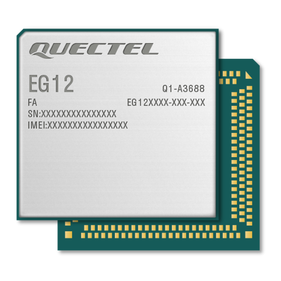
7.3. Top and Bottom Views of the Module Figure 47: Top View of the Module Figure 48: Bottom View of the Module NOTE These are renderings of EG12. For authentic appearance, please refer to the module that you receive from Quectel. EG12_Hardware_Design 89 / 97... -
Page 91: Storage, Manufacturing And Packaging
LTE-A Module Series EG12 Hardware Design Storage, Manufacturing and Packaging 8.1. Storage EG12 is stored in a vacuum-sealed bag. It is rated at MSL 3, and its storage restrictions are listed below. 1. Shelf life in vacuum-sealed bag: 12 months at <40º C/90%RH. After the vacuum-sealed bag is opened, devices that will be subjected to reflow soldering or other high temperature processes must be: ... -
Page 92: Manufacturing And Soldering
LTE-A Module Series EG12 Hardware Design 8.2. Manufacturing and Soldering Push the squeegee to apply the solder paste on the surface of stencil, thus making the paste fill the stencil openings and then penetrate to the PCB. The force on the squeegee should be adjusted properly so as to produce a clean stencil surface on a single pass. -
Page 93: Packaging
LTE-A Module Series EG12 Hardware Design Reflow Zone Max slope 2 to 3° C/sec Reflow time (D: over 220° C) 40 to 60 sec Max temperature 238° C ~ 245° C Cooling down slope 1 to 4° C/sec Reflow Cycle Max reflow cycle 8.3. - Page 94 LTE-A Module Series EG12 Hardware Design Figure 51: Reel Specifications EG12_Hardware_Design 93 / 97...
-
Page 95: Appendix A References
LTE-A Module Series EG12 Hardware Design Appendix A References Table 49: Related Documents Document Name Remark Quectel_UMTS<E_EVB_R2.0_User_Guide UMTS<E EVB R2.0 User Guide Quectel_EM12&EG12&EG18_AT_Commands_ AT Commands Manual for EM12, EG12 Manual and EG18 Quectel_EM12&EG12&EG18_GNSS_Application GNSS Application Note for EM12, EG12 _Note and EG18 Quectel_Module_Secondary_SMT_User_Guide Module Secondary SMT User Guide... - Page 96 LTE-A Module Series EG12 Hardware Design DC-HSPA+ Dual-carrier High Speed Packet Access DFOTA Delta Firmware Upgrade Over The Air Downlink Discontinuous Reception Data Terminal Ready Discontinuous Transmission Enhanced Full Rate Electrostatic Discharge Full Rate GLObalnaya NAvigatsionnaya Sputnikovaya Sistema, the Russian Global GLONASS Navigation Satellite System GMSK...
- Page 97 LTE-A Module Series EG12 Hardware Design Password Authentication Protocol Printed Circuit Board Protocol Data Unit Point-to-Point Protocol Quadrature Amplitude Modulation QPSK Quadrature Phase Shift Keying Radio Frequency RHCP Right Hand Circularly Polarized Receive SGMII Serial Gigabit Media Independent Interface SIMO Single Input Multiple Output Short Message Service Time Division Duplexing...
- Page 98 LTE-A Module Series EG12 Hardware Design Absolute Maximum Input Voltage Value Absolute Minimum Input Voltage Value Maximum Output High Level Voltage Value Minimum Output High Level Voltage Value Maximum Output Low Level Voltage Value Minimum Output Low Level Voltage Value VSWR Voltage Standing Wave Ratio EG12_Hardware_Design...
Need help?
Do you have a question about the EG12 Series and is the answer not in the manual?
Questions and answers