
Related Manuals for Quectel EG915Q-NA


Summary of Contents for Quectel EG915Q-NA
- Page 1 EG915Q-NA Hardware Design LTE Standard Module Series Version: 1.0 Date: 2023-02-07 Status: Released...
- Page 2 LTE Standard Module Series At Quectel, our aim is to provide timely and comprehensive services to our customers. If you require any assistance, please contact our headquarters: Quectel Wireless Solutions Co., Ltd. Building 5, Shanghai Business Park Phase III (Area B), No.1016 Tianlin Road, Minhang District, Shanghai...
- Page 3 Except as otherwise set forth herein, nothing in this document shall be construed as conferring any rights to use any trademark, trade name or name, abbreviation, or counterfeit product thereof owned by Quectel or any third party in advertising, publicity, or other aspects.
-
Page 4: Safety Information
Manufacturers of the cellular terminal should notify users and operating personnel of the following safety information by incorporating these guidelines into all manuals of the product. Otherwise, Quectel assumes no liability for customers’ failure to comply with these precautions. -
Page 5: About The Document
LTE Standard Module Series About the Document Revision History Version Date Author Description 2022-11-28 Lex LI/Lena HUANG Creation of the document 2023-02-07 Lex LI/Barry DENG First official release EG915Q-NA_Hardware_Design 4 / 72... -
Page 6: Table Of Contents
LTE Standard Module Series Contents Safety Information ............................3 About the Document ........................... 4 Contents ............................... 5 Table Index ..............................7 Figure Index ..............................9 Introduction ............................11 1.1. Special Marks .......................... 11 Product Overview ..........................12 2.1. Frequency Bands ........................12 2.2. - Page 7 LTE Standard Module Series 4.6. ADC Interfaces ........................42 4.7. SPI Interface* ........................... 43 4.8. Camera SPI Interface* ......................43 4.9. GRFC Interfaces* ........................44 4.10. Control Signals ........................44 4.10.1. W_DISABLE#* ........................ 45 4.11. Indication Signals ........................45 4.11.1. Network Status Indication ....................46 4.11.2.
- Page 8 Table 28: Operating Frequency of EG915Q-NA (Unit: MHz) ..............48 Table 29: RF Transmitting Power ........................ 49 Table 30: Conducted RF Receiver Sensitivity of EG915Q-NA (Unit: dBm) ..........49 Table 31: Requirements for Antenna Design ....................53 Table 32: Absolute Maximum Ratings ......................55 Table 33: Module’s Power Supply Ratings ......................
- Page 9 LTE Standard Module Series Table 42: Plastic Reel Dimension Table (Unit: mm) ..................67 Table 43: Related Documents........................69 Table 44: Terms and Abbreviations ......................69 EG915Q-NA_Hardware_Design 8 / 72...
- Page 10 LTE Standard Module Series Figure Index Figure 1: Functional Diagram ........................15 Figure 2: Pins Assignment (Top View) ......................16 Figure 3: Power Consumption During Sleep Mode ..................23 Figure 4: Block Diagram of UART Application in Sleep Mode ..............23 Figure 5: Block Diagram of Application with USB Remote Wakeup Function in Sleep Mode ....
- Page 11 LTE Standard Module Series Figure 42: Plastic Reel Dimension Drawing ....................67 Figure 43: Mounting Direction ........................67 Figure 44: Packaging Process ........................68 EG915Q-NA_Hardware_Design 10 / 72...
-
Page 12: Introduction
LTE Standard Module Series Introduction This document describes the EG915Q-NA features, performance, and air interfaces and hardware interfaces connected to your applications. The document provides a quick insight into interface specifications, RF performance, electrical and mechanical specifications, and other module information, as well. -
Page 13: Product Overview
LTE Standard Module Series Product Overview EG915Q-NA is an SMD module with compact packaging, which is engineered to meet most of the demands of M2M and IoT applications, such as asset management, commercial telematics, payment, RMAC (Remote Monitoring and Control applications), security and automation, smart metering and smart grid. -
Page 14: Key Features
Use: network connectivity status indication ⚫ Complies with the AT commands defined in 3GPP TS 27.007 and ⚫ AT Commands 3GPP TS 27.005 ⚫ Complies with Quectel enhanced AT commands ⚫ Main antenna interface (ANT_MAIN) Antenna Interface ⚫ 50 Ω characteristic impedance EG915Q-NA_Hardware_Design... - Page 15 LTE Standard Module Series Transmitting Power ⚫ LTE-FDD: Class 3 (23 dBm ± 2 dB) ⚫ Complies with 3GPP Rel-14 FDD ⚫ Max. LTE category: Cat 1 bis ⚫ 1.4/3/5/10/15/20 MHz RF bandwidth ⚫ DL modulations: QPSK, 16QAM and 64QAM LTE Features ⚫...
-
Page 16: Functional Diagram
LTE Standard Module Series 2.3. Functional Diagram The functional diagram illustrates the following major functional parts: ⚫ Power management Baseband part ⚫ ⚫ Radio frequency part ⚫ Peripheral interfaces ANT_MAIN Switch Duplex VBAT_RF 26 MHz UARTs Baseband RF Transceiver VBAT_BB PMIC and Subsystem PWRKEY... -
Page 17: Pin Assignment
LTE Standard Module Series 2.4. Pin Assignment PSM_IND RESER VED ADC1 RESER VED RESER VED RESERVED RESER VED PCM_CL K USIM_CLK RESER VED RESER VED RESER VED RESERVED CAM_PWDN PCM_SYNC USIM_DATA RESER VED PCM_DIN RESERVED USIM_RST CAM_SPI_DATA1 CAM_SPI_CLK PCM_DOUT USIM_VDD RESERVED RESER VED RESER VED... -
Page 18: Pin Description
LTE Standard Module Series 2.5. Pin Description The following table shows the pin descriptions. DC characteristics include power domain, rate current, etc. Table 5: Parameter Definition Parameters Descriptions Analog Input Analog Input/Output Digital Input Digital Output Digital Input/Output Power Input Power Output Table 6: Pin Description Power Supply... - Page 19 LTE Standard Module Series Pin Name Pin No. Description Comment Characteristic PWRKEY Turns on/off the module Active low. Active low. max = 0.5 V Test points are RESET_N Resets the module recommended to be reserved if unused. Indication Signals Pin Name Pin No.
- Page 20 LTE Standard Module Series USIM_RST USIM card reset If unused, keep it USIM card hot-plug USIM_DET VDD_EXT open. detect Main UART Pin Name Pin No. Description Comment Characteristic Connect to DTE’s DTE clear to send signal CTS. MAIN_CTS from DCE If unused, keep it open.
- Page 21 LTE Standard Module Series PCM_SYNC PCM data frame sync PCM_CLK PCM clock If unused, keep them VDD_EXT open. PCM_DIN PCM data input PCM_DOUT PCM data output RF Antenna Interface Pin Name Pin No. Description Comment Characteristic ANT_MAIN Main antenna interface 50 Ω...
-
Page 22: Evb Kit
Keep these pins RESERVED 116–126 open. 2.6. EVB Kit To help you develop applications with the module, Quectel supplies an evaluation board (UMTS<E EVB) with accessories to control or test the module. For more details, see document [1]. EG915Q-NA_Hardware_Design 21 / 72... -
Page 23: Operating Characteristics
LTE Standard Module Series Operating Characteristics 3.1. Operating Modes Table 7: Operating Modes Overview Modes Descriptions Software is active. The module is registered on the network but has Idle Full Functionality no data interaction with the network. Network connection is ongoing. Power consumption is decided by Mode Data network setting and data rate. -
Page 24: Sleep Mode
LTE Standard Module Series 3.2. Sleep Mode With DRX technology, power consumption of the module will be reduced to a minimal level. DRX OFF ON Run Time Figure 3: Power Consumption During Sleep Mode 3.2.1. UART Application Scenario If the module communicates with the host via main UART, both the following preconditions should be met to set the module to sleep mode: ⚫... -
Page 25: Usb Application Scenarios
LTE Standard Module Series 3.2.2. USB Application Scenarios* For the two situations (“USB application with USB remote wakeup function” and “USB application with USB suspend/resume and MAIN_RI function”) below, three preconditions must be met to set the module to sleep mode: Execute AT+QSCLK=1. -
Page 26: Usb Application Without Usb Suspend Function
LTE Standard Module Series Module Host USB_VBUS USB_DP USB_DP USB_DM USB_DM GPIO AP_READY MAIN_RI EINT Figure 6: Sleep Mode Application with USB Suspend/Resume and MAIN_RI ⚫ Sending data to the module through USB will wake up the module. ⚫ When the module has a URC to report, the module will wake up the host through MAIN_RI signal. See Chapter 4.11.3 for details about MAIN_RI behavior. -
Page 27: Airplane Mode
LTE Standard Module Series NOTE Pay attention to the level match shown in the dotted line between the module and the host. 3.3. Airplane Mode When the module enters airplane mode, the RF function will be disabled, and all AT commands correlative with RF function will be inaccessible. -
Page 28: Reference Design For Power Supply
LTE Standard Module Series 3.4.2. Reference Design for Power Supply Power design for the module is essential. The power supply of the module should be able to provide sufficient current of 2 A at least. If the voltage difference between input voltage and the supply voltage is small, it is suggested to use an LDO;... -
Page 29: Turn On
LTE Standard Module Series recommended to add a TVS with V = 4.7 V, low clamping voltage and high reverse peak pulse current Ipp at the front end of the power supply. VBAT VBAT_RF VBAT_BB 100 nF 33 pF 10 pF 100 µF 100 nF 33 pF 10 pF 100 µF... - Page 30 LTE Standard Module Series 500 ms PWRKEY Turn on pulse 4.7K GPIO Module Figure 10: Reference Design of Turn On with Driving Circuit Another way to control the PWRKEY is using a keystroke directly. When pressing the keystroke, an electrostatic strike may be generated from finger. Therefore, you should place a TVS component near the keystroke for ESD protection.
-
Page 31: Turn Off
LTE Standard Module Series NOTE 1 <10 ms 500 ms VBAT V 0.1 V PWRKEY 0.5 V About 40 ms VDD_EXT Connect USB_BOOT to VDD_EXT before the module is turned o n , and then the module will enter the emergency download mode when it is turned on. -
Page 32: Turn Off With At Command
LTE Standard Module Series VBAT 650 ms PWRKEY STATUS Module Power-down procedure Running Status Figure 13: Power-down Timing with PWRKEY 3.6.2. Turn Off with AT Command For proper shutdown procedure, execute AT+QPOWD, which has similar timing and effect as turning off the module through driving PWRKEY low. - Page 33 LTE Standard Module Series Table 10: Pin Description of RESET_N Pin Name Pin No. Description Comment Active low. RESET_N Reset the module Test points are recommended to be reserved if unused. The recommended circuit for reset function is similar to the PWRKEY control circuit. You can use an open drain/collector driver or a button to control RESET_N and PWRKEY pins.
- Page 34 LTE Standard Module Series VBAT ≥ 500 ms PWRKEY ≤ 0.5 V ≥ 300 ms RESET_N ≤ 0.5 V Module Running Resetting Restart Status Figure 16: Reset Timing NOTE 1. In reset timing, pull down PWRKEY when RESET_N is at low level. 2.
-
Page 35: Application Interfaces
LTE Standard Module Series Application Interfaces 4.1. USB Interface The module provides one integrated Universal Serial Bus (USB) interface which complies with the USB 2.0 specifications and supports high-speed (480 Mbps) and full-speed (12 Mbps) for USB 2.0. The module only supports USB slave mode. The USB interface can be used for AT command communication, data transmission, software debugging, firmware upgrade and the output of partial logs. -
Page 36: Usb_Boot
LTE Standard Module Series It is recommended to add a common-mode choke L1 in series between MCU and the module to suppress EMI spurious transmission. Meanwhile, it is also suggested to add R1 and R2 in series between the module and test points for debugging. These resistors are not mounted by default. To ensure the signal integrity of USB 2.0 data transmission, you should place L1, R1 and R2 close to the module, and keep these resistors close to each other. - Page 37 LTE Standard Module Series Module VDD_EXT Test points 4.7K USB_BOOT TVS should be placed close to test points. Figure 18: Reference Design of USB_BOOT NOTE 1 VBAT 500 ms PWRKEY 0.5 V About 40ms USB_BOOT can be pulled up to 1.8 V before VDD_EXT VDD_EXT is powered up, and the module will enter emergency download mode when it is turned...
-
Page 38: Usim Interface
LTE Standard Module Series 4.3. USIM Interface The USIM interface meets ETSI and IMT-2000 requirements. Either 1.8 V or 3.0 V USIM card is supported. Table 13: Pin Description of USIM Interface Pin Name Pin No. Description Comment Either 1.8 V or 3.0 V USIM card is USIM_VDD USIM card power supply supported and can be identified... - Page 39 LTE Standard Module Series If the function of USIM card hot-plug is not needed, keep USIM_DET disconnected. A reference design for USIM interface with a 6-pin USIM card connector is illustrated in the following figure. USIM_VDD 100 nF USIM Card Connector USIM_VDD USIM_RST Module...
-
Page 40: Uart Interfaces
LTE Standard Module Series 4.4. UART Interfaces The module serves as DCE (Data Communication Equipment), which is connected in the traditional DCE-DTE (Data Terminal Equipment) mode. The module provides two UART Interfaces. Table 14: UART Information (Unit: bps) UART Types Supported Baud Rates Default Baud Rates Functions... - Page 41 LTE Standard Module Series VCCA VCCB VDD_EXT VDD_MCU 0.1 μF 0.1 μF 120K MAIN_RI RI_MCU MAIN_DCD DCD_MCU Level-shifting CTS_MCU MAIN_CTS Chip MAIN_RTS RTS_MCU MAIN_DTR DTR_MCU MAIN_TXD RXD_MCU MAIN_RXD TXD_MCU Figure 22: Reference Design of UART with Level-shifting Chip Another example of level-shifting circuit is shown as below. For the design of circuits in dotted lines, see that shown in solid lines, but pay attention to the direction of the connection.
-
Page 42: Pcm And I2C Interfaces
LTE Standard Module Series 4.5. PCM and I2C Interfaces* The module provides one Pulse Code Modulation (PCM) digital interface and one I2C interface. Table 16: Pin Description of PCM and I2C Interfaces Pin Name Pin No. Description Comment PCM_SYNC PCM data frame sync PCM_CLK PCM clock If unused, keep them open. -
Page 43: Adc Interfaces
LTE Standard Module Series 4.6. ADC Interfaces The module provides two Analog-to-Digital Converter (ADC) interfaces. To improve the accuracy of ADC, surround the trace of ADC with ground. Table 17: Pin Description of ADC Interfaces Pin Name Pin No. Description Comment ADC0 General-purpose ADC interface... -
Page 44: Spi Interface
LTE Standard Module Series 4.7. SPI Interface* The module provides one SPI interface with a maximum clock frequency up to 25.6 MHz. Table 19: Pin Description of SPI Interface Pin Name Pin No. Description Comment SPI_CLK SPI clock SPI_CS SPI chip selection If unused, keep them open. -
Page 45: Grfc Interfaces
LTE Standard Module Series Table 20: Pin Description of Camera SPI Interface Pin Name Pin No. Description Comment CAM_MCLK Master clock of the camera CAM_SPI_CLK Camera SPI clock CAM_SPI_DATA0 Camera SPI data bit 0 If unused, keep them CAM_SPI_DATA1 Camera SPI data bit 1 open. -
Page 46: W_Disable
W_DISABLE# is a control function for airplane mode, which is disabled in software by default. It can be enabled through AT+QCFG="airplanecontrol",1. For the details of this command, please contact Quectel Technical Support. 4.11. Indication Signals Table 24: Pin Description of Indication Signals Pin Name Pin No. -
Page 47: Network Status Indication
LTE Standard Module Series 4.11.1. Network Status Indication The module provides one network status indication pins: the NET_STATUS for the module’s network operation status indication, which can drive corresponding LEDs. Table 25: Network Status Indication Pin Level and Module Network Status Pin Name NET_STATUS Level Status Module Network Status... -
Page 48: Main_Ri
AT+QCFG= “risignaltype”, “physical” can be used to configure MAIN_RI behavior. No matter on which port a URC information is presented, the URC information will trigger the behavior of the MAIN_RI. For the details of AT+QCFG, please contact Quectel Technical Support. NOTE The AT+QURCCFG allows you to set the main UART, USB AT port or USB modem port as the URC information output port. -
Page 49: Rf Specifications
Table 27: Pin Description of Cellular Antenna Interface Pin Name Pin No. Description Comment ANT_MAIN Main antenna interface 50 Ω impedance. Table 28: Operating Frequency of EG915Q-NA (Unit: MHz) Operating Frequency Transmit Receive LTE-FDD B2 1850–1910 1930–1990 LTE-FDD B4 1710–1755 2110–2155... -
Page 50: Tx Power
Max. RF Output Power Min. RF Output Power LTE-FDD bands 23 dBm ± 2 dB < -39 dBm 5.1.3. Rx Sensitivity Table 30: Conducted RF Receiver Sensitivity of EG915Q-NA (Unit: dBm) Receiver Sensitivity (Typ.) Frequency Bands 3GPP (SIMO) Primary LTE-FDD B2 (10 MHz) -98 dBm -94.3 dBm... -
Page 51: Reference Design
LTE Standard Module Series 5.1.4. Reference Design Main Antenna ANT_MAIN Module Figure 28: Reference Design of Main Antenna NOTE Use a π-type matching circuit for the antenna interface for better cellular performance and for the ease of debugging. Capacitors are not mounted by default. Place the π-type matching components (R1 &... - Page 52 LTE Standard Module Series Figure 29: Microstrip Design on a 2-layer PCB Figure 30: Coplanar Waveguide Design on a 2-layer PCB Figure 31: Coplanar Waveguide Design on a 4-layer PCB (Layer 3 as Reference Ground) EG915Q-NA_Hardware_Design 51 / 74...
- Page 53 LTE Standard Module Series Figure 32: Coplanar Waveguide Design on a 4-layer PCB (Layer 4 as Reference Ground) To ensure RF performance and reliability, follow the principles below in RF layout design: Use an impedance simulation tool to accurately control the characteristic impedance of RF traces to ⚫...
-
Page 54: Antenna Design Requirements
LTE Standard Module Series 5.3. Antenna Design Requirements Table 31: Requirements for Antenna Design Antenna Types Requirements ⚫ VSWR: ≤ ⚫ Efficiency: > 30 % ⚫ Gain: 1 dBi ⚫ Max. input power: 50 W ⚫ Input impedance: 50 Ω ⚫... - Page 55 LTE Standard Module Series Figure 34: Specifications of Mated Plugs The following figure describes the space factor of mated connectors. Figure 35: Space Factor of Mated Connectors (Unit: mm) For more details, please visit http://www.hirose.com. EG915Q-NA_Hardware_Design 54 / 74...
-
Page 56: Electrical Characteristics & Reliability
LTE Standard Module Series Electrical Characteristics & Reliability 6.1. Absolute Maximum Ratings Table 32: Absolute Maximum Ratings Parameters Min. Max. Unit Voltage at VBAT_RF & VBAT_BB -0.3 Voltage at USB_VBUS -0.3 5.25 Voltage at digital pins -0.3 6.2. Power Supply Ratings Table 33: Power Supply Ratings Parameters Descriptions... -
Page 57: Power Consumption
LTE-FDD B66 N ⚫ OTE The power consumption data above is for reference only, which may vary among different modules. For detailed information, contact Quectel Technical Support for the power consumption test report of the specific module. EG915Q-NA_Hardware_Design 56 / 74... -
Page 58: Digital I/O Characteristics
LTE Standard Module Series 6.4. Digital I/O Characteristics Table 35: VDD_EXT I/O Characteristics (Unit: V) Parameters Descriptions Min. Max. High-level input voltage Low-level input voltage -0.3 High-level output voltage 1.35 Low-level output voltage 0.45 Table 36: USIM Low-voltage I/O Characteristics (Unit: V) Parameters Descriptions Min. -
Page 59: Esd Protection
LTE Standard Module Series 6.5. ESD Protection Static electricity occurs naturally and it may damage the module. Therefore, applying proper ESD countermeasures and handling methods is imperative. For example, wear anti-static gloves during the development, production, assembly and testing of the module; add ESD protection components to the ESD sensitive interfaces and points in the product design. -
Page 60: Mechanical Information
LTE Standard Module Series Mechanical Information This chapter describes the mechanical dimensions of the module. All dimensions are measured in millimeter (mm), and the dimensional tolerances are ± 0.2 mm unless otherwise specified. 7.1. Mechanical Dimensions Figure 36: Top and Side Dimensions (Unit: mm) EG915Q-NA_Hardware_Design 59 / 74... - Page 61 LTE Standard Module Series Figure 37: Bottom Dimensions (Bottom View, Unit: mm) N ⚫ OTE The package warpage level of the module conforms to the JEITA ED-7306 standard. EG915Q-NA_Hardware_Design 60 / 74...
-
Page 62: Recommended Footprint
LTE Standard Module Series 7.2. Recommended Footprint Figure 38: Recommended Footprint (Unit: mm) NOTE Keep at least 3 mm between the module and other components on the motherboard to improve soldering quality and maintenance convenience. EG915Q-NA_Hardware_Design 61 / 74... -
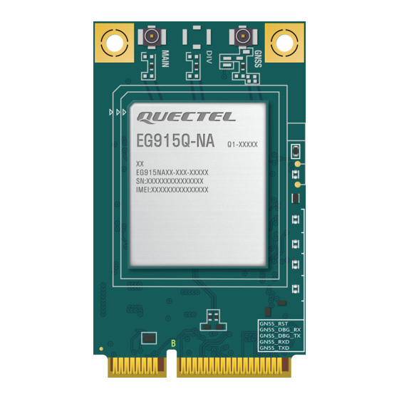
Page 63: Top And Bottom Views
Figure 39: Top and Bottom Views of the Module NOTE Images above are for illustration purpose only and may differ from the actual module. For authentic appearance and label, please refer to the module received from Quectel. EG915Q-NA_Hardware_Design 62 / 74... -
Page 64: Storage, Manufacturing & Packaging
LTE Standard Module Series Storage, Manufacturing & Packaging 8.1. Storage Conditions The module is provided with vacuum-sealed packaging. MSL of the module is rated as 3. The storage requirements are shown below. 1. Recommended Storage Condition: the temperature should be 23 ± 5 ° C and the relative humidity should be 35–60 %. -
Page 65: Manufacturing And Soldering
LTE Standard Module Series NOTE 1. To avoid blistering, layer separation and other soldering issues, extended exposure of the module to the air is forbidden. 2. Take out the module from the package and put it on high-temperature-resistant fixtures before baking. - Page 66 5. Avoid using ultrasonic technology for module cleaning since it can damage crystals inside the module. 6. Due to the complexity of the SMT process, contact Quectel Technical Supports in advance for any situation that you are not sure about, or any process (e.g. selective wave soldering, ultrasonic soldering) that is not mentioned in document [4].
-
Page 67: Packaging Specification
LTE Standard Module Series 8.3. Packaging Specification This chapter describes only the key parameters and process of packaging. All figures below are for reference only. The appearance and structure of the packaging materials are subject to the actual delivery. The module adopts carrier tape packaging and details are as follow: 8.3.1. -
Page 68: Plastic Reel
LTE Standard Module Series 8.3.2. Plastic Reel Figure 42: Plastic Reel Dimension Drawing Table 42: Plastic Reel Dimension Table (Unit: mm) øD1 øD2 44.5 Mounting Direction 8.3.3. Figure 43: Mounting Direction EG915Q-NA_Hardware_Design 67 / 74... -
Page 69: Packaging Process
LTE Standard Module Series 8.3.4. Packaging Process Place the module into the carrier tape and use the cover tape to cover it; then wind the heat-sealed carrier tape to the plastic reel and use the protective tape for protection. 1 plastic reel can load 250 modules. Place the packaged plastic reel, 1 humidity indicator card and 1 desiccant bag into a vacuum bag, vacuumize it. -
Page 70: Appendix References
LTE Standard Module Series Appendix References Table 43: Related Documents Document Name [1] Quectel_UMTS<E_EVB_User_Guide [2] Quectel_EG800Q-EU&EG915Q-NA_AT_Commands_Manual [3] Quectel_RF_Layout_Application_Note [4] Quectel_Module_SMT_Application_Note Table 44: Terms and Abbreviations Abbreviation Description 3GPP 3rd Generation Partnership Project Analog-to-Digital Converter Bits Per Second CHAP Challenge Handshake Authentication Protocol CMUX Connection MUX Clear To Send... - Page 71 LTE Standard Module Series Electrostatic Discharge Frequency Division Duplex FILE File Protocol File Transfer Protocol FTPS FTP over SSL GRFC General RF Control High Band HTTP Hypertext Transfer Protocol HTTPS Hypertext Transfer Protocol Secure Inter-Integrated Circuit Input/Output IMT-2000 International Mobile Telecommunications 2000 Low Band Light Emitting Diode Land Grid Array...
- Page 72 LTE Standard Module Series Pulse Code Modulation Personal Digital Assistant Protocol Data Unit PING Packet Internet Groper Point-to-Point Protocol Quadrature Amplitude Modulation QPSK Quadrature Phase Shift Keying Ring Indicator Radio Frequency Receive Surface Mount Device Short Message Service Secure Sockets Layer Serial Peripheral Interface Transmission Control Protocol Transmit...
- Page 73 Working Peak Reverse Voltage VSWR Voltage Standing Wave Ratio Product Marketing Name:Quectel EG915Q-NA FCC Certification Requirements. According to the definition of mobile and fixed device is described in Part 2.1091(b), this device is a mobile device. And the following conditions must be met: 1.
- Page 74 LTE Standard Module Series 5. This module must not transmit simultaneously with any other antenna or transmitter 6. The host end product must include a user manual that clearly defines operating requirements and conditions that must be observed to ensure compliance with current FCC RF exposure guidelines. For portable devices, in addition to the conditions 3 through 6 described above, a separate approval is required to satisfy the SAR requirements of FCC Part 2.1093 If the device is used for other equipment that separate approval is required for all other operating configurations,...
- Page 75 LTE Standard Module Series clairement visible en tout temps lorsqu'il est installédans le produit hôte; sinon, le produit hôte doit porter une étiquette indiquant le numéro de certification d'Innovation, Sciences et Développement économique Canada pour le module, précédé du mot « Contient» ou d'un libellé semblable exprimant la mê me signification, comme suit: "Contient IC: 10224A-023EG915QNA "...
Need help?
Do you have a question about the EG915Q-NA and is the answer not in the manual?
Questions and answers