Table of Contents
Advertisement
Quick Links
ORDER NO. KMS0303678C3
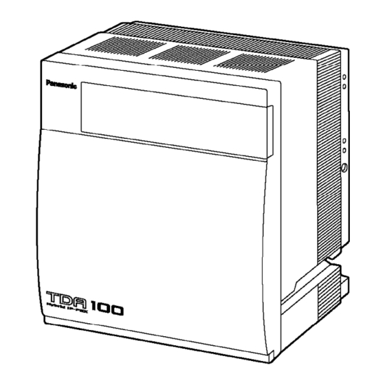
Hybrid IP-PBX
KX-TDA100AL
(for Australia)
2003 Panasonic Communications Co., Ltd. All rights reserved.
Unauthorized copying and distribution is a violation of law.
IMPORTANT INFORMATION ABOUT LEAD FREE, (PbF), SOLDERING
If lead free solder was used in the manufacture of this product the printed circuit boards will be
marked PbF.
Standard leaded, (Pb), solder can be used as usual on boards without the PbF mark.
When this mark does appear please read and follow the special instructions described in this
1
Advertisement
Table of Contents

Related Manuals for Panasonic KX-TDA100AL


Summary of Contents for Panasonic KX-TDA100AL
- Page 1 Hybrid IP-PBX KX-TDA100AL (for Australia) 2003 Panasonic Communications Co., Ltd. All rights reserved. Unauthorized copying and distribution is a violation of law. IMPORTANT INFORMATION ABOUT LEAD FREE, (PbF), SOLDERING If lead free solder was used in the manufacture of this product the printed circuit boards will be marked PbF.
-
Page 2: About Lead Free Solder (Pbf: Pb Free)
manual on the use of PbF and how it might be permissible to use Pb solder during service and repair work. 1. ABOUT LEAD FREE SOLDER (PbF: Pb free) Note: In the information below, Pb, the symbol for lead in the periodic table of elements, will refer to standard solder or solder that contains lead. -
Page 3: How To Recognize That Pb Free Solder Is Used
Please check the manufac turer’s specific instructions for the melting points of their products and any precautions for using their product with other materials. The following lead free (PbF) solder wire sizes are recommended for service of this product: 0.3mm, 0.6mm and 1.0mm. 1.2. -
Page 4: Insulation Resistance Test
damage is evident. 4. After servicing, be sure to restore the lead dress, insulation barriers, insulation papers, shields, etc. 5. Before returning the serviced equipment to the customer, be sure to perform the following insulation resistance test to prevent the customer from being exposed to shock hazards. -
Page 5: Specifications
1. Danger of explosion if battery is incorrectly replaced. Replace only with the same or equivalent type recommended by the manufacturer. Dispose of used batteries according to the manufacturer’s Instructions. 2. The lithium battery is a critical component (type No.CR23541). Please observe for the proper polarity and the exact location when replacing it and soldering the replacement lithium battery in. -
Page 6: System Capacity
Serial Interface Port RS-232C 1 (max 115.2 kbps) Extension Connection Cable 1 pair wire (T, R) 1-pair wire (D1, D2) or 2-pair wire (T, R, D1, D2) 2-pair wire (T, R, D1, D2) DSS Consoles and Add-on Key 1-pair wire (D1, D2) Module Dimension KX-TDA100... - Page 7 Card Type KX-TDA100 Trunk Card *1 Extension Card Total *1 One T1, E1, PRI30 and PRI23 card counts as 2 cards. Note: - For each card, a maximum number that can be installed in the Hybrid IP-PBX is listed in "Installation Manual". - Any card that exceeds the capacity of the Hybrid IP-PBX will be ignored.
-
Page 8: System Overview
Equipment Type Load Figure DPT (T76xx series and T7560, T7565) Other DPT/APT/DSS Console Extension Card *1 DHLC8 SLC8 SLC16 MSLC16 ISDN Extension Voice Mail *1 Only the extension cards that can support SLTs count for the load figures. PSU Capability Each PSU supports a different amount of load figures. -
Page 9: System Components
5.2. SYSTEM COMPONENTS... - Page 10 Model Card Name Description Shelves Basic Shelf TDA100AL Main Processing Main Processing Card Card MPR Option Card KX- Remote Card TDA0196XJ CO Line Cards LCO8 8-Port Analogue Trunk Card TDA0180AL LCOT16 16-Port Analogue Trunk Card E&M8 8-Port E &M Trunk Card TDA0181AL E-1 Trunk Card CID/PAY8...
- Page 11 KX-A258XJ Blank Slot Cover KX-T30865X Doorphone Available Telephones The Hybrid IP-PBX supports all of the Panasonic X-T7xxx and KX-TD7xxx series: - Digital/Analog proprietary telephones (e.g., KX-T7625, KX-T7630, KX-T7633, KX-T7636) - Portable stations (e.g., KX-TD7590) - DSS consoles (e.g., KX-T7640) - Single line telephones (e.g., KX-T7710)
-
Page 12: System Connection Diagram
- There are some optional service cards and features that are not available for certain countries/areas. Consult your authorized Panasonic dealer for detailed instructions. - The power supply capacity of the Hybrid IP-PBX may differ from the values described in this manual depending on the model number.Please consult your dealer for detailed information. -
Page 14: Name And Locations
*Only 1 Server PC can be connected to the Hybrid IP-PBX.Two or more Server PCs cannot be used simultaneously. 6. NAME AND LOCATIONS... - Page 15 - Null slot : Null slot is not available for any optional service card. - RUN Indicator :...
- Page 16 Shows the system normally working by green light. - ALARM Indicator : Shows the system detected some obstacles. - RS-232C Port : They work as system programing/administration interface port, SMDR information output port, computer telephony integration port. Note: - Line capacity of this cabinet is up to 108 ports. - These limitation of line capacity is checked at installation of slot assignment.
- Page 17 1. Remove the Lib by sliding it in the direction of the arrow 1. 2. This will be removed if the user attaches the Pad Lock as shown in a Fig.1. 3. Loosen the Screw. 4. Front Cover is removed in the direction of an arrow 2.
-
Page 18: Disassembly Instruction (Back Board)
5. Loosen the two Screws. 6. Remove the MPR Card. 7.2. DISASSEMBLY INSTRUCTION (BACK BOARD) 1. Remove four Screws (A). 2. Remove the Left Side Cover and the Right Side Cover. - Page 19 3. Remove the Hook. And remove the Top Cover. 4. Remove nine Screws (B). 5. Remove the Back Cover.
- Page 20 6. Remove the RS-232C Connector and LED Connector from the Back Board 1. 7. Remove eight Screws (C). 8. Remove the Back Board 1. 9. Remove the LED Connector from the Back Board 2. 10. Remove the Screw (C). 11. Remove the Back Board 2. 8.
-
Page 21: System Control
through the inter-processor communication system. POWER detects the voltage drop of the AC input and the DC output and transfers it to MPR. 8.1.1. MPR Card This card is the main control section of this unit. It controls all the cards mounted on the free slots, and communication of RS-232C ports. - Page 22 8.2.2. Voice (TDM Highway) Bus Block Diagram...
- Page 23 8.2.3. Voice Bus Logical Assignment...
-
Page 24: Back Board Signal Connection Diagram
In the line card, the CT_D line number, which is output in accordance with the inserted slot, and the time slot are assigned on a software base. For the detail of output slot for each card, refer to the service manual of card. 8.2.4. - Page 25 8.3.2. EC Bus System Connection Diagram...
- Page 26 8.3.3. System Control and Analog Signal Connection Diagram...
- Page 27 8.3.4. Power Supply System Connection Diagram...
- Page 28 9. MPR CARD CIRCUIT OPERATION 9.1. MPR CARD 9.1.1. Outline 1) Function - System Control - Circuit Switching (includes gain adjustment function) - Conference Call (3 people x 8 ~ 8 people x 3) - MOH - PAGING - Clock 2) Configuration - Power Supply: DC/DC Converter - CPU: HITACHI SH7709S (133MHz)
- Page 29 +5VRMT unused (for remote card) +5V (for RS-232C driver/receiver) 9.1.2. Description of Each Part...
- Page 31 LED light (BATALM): Turns on to indicate the dropping of the lithium battery voltage (less than 2.8V). LED light (SD ACCES): Turns on when the SD card is accessing. SD card slot: Mounts the system program SD card. Reset Switch: Press at the system reset. System Initialize Switch: On default startup, set the switch to the "SYSTEM INITIALIZE"...
- Page 32 on-hold input 1 system and exclusively the internal music on-hold output. - Power block This consists of DC/DC converter circuit and various regulators. 9.1.4.2. Detail of Block Description - CPU block Configuration: IC101 (CPU), IC107 (reset IC), IC103 (spread clock IC), X101 (CPU source clock), X102 (clocking clock) and so on.
- Page 33 Signal Name Function +15VIN +15V DC +15V For Circuit +15V DC MOH +9.4V For Driver IC +9.4V DC RS-232C For Driver IC +5V DC RS-232C +5VRMT Reserve 3.3V_BB +3.3V DC For pull-up of back board signal line +3.3VB +3.3V DC Backup by a battery For SRAM (IC301, IC302) backup +3.3V...
- Page 34 Signal Name Function nCS_SRAM0 Chip Select for SRAM0: CS signal for IC301 nCS_SRAM1 Chip Select for SRAM1: CS signal for IC302 nCS_USB Chip Select for USB I/F nCTS2 Clear To Send from RS-232C connector CTS_RMT Clear to Send: Flow signal for modem CT_C8 Clock8.192MHz clock outputted from PLL master CT_D[0] -[7]...
- Page 35 Signal Name Function FSEL0 Signal switching the Flash Memory address of the MEX card. FSEL0 is set by hard jumper.L: The number of Flash Memory chips on the MPR is 1pc. H: The number GAIN0-1 Gain: Gain adjustment signal for the RMT card (Reserve) HALT This alarms the occurrence of the declined DC voltage to line card.
- Page 36 Signal Name Function POWTYPE S Power Supply attached M Power Supply attached L Power Supply attached nPRS_MEX Press MEX: Information of MEX Card Attachment L: Attached, H: Not attached nPRS_RMT Press RMT: Information of RMT Card Attachment L: Attached, H: Not attached nPRS_SDB Press SD card: Information of SD Card Attachment L: Attached, H: Not attached nRAS3L...
- Page 37 Signal Name Function VBUS Bit indicating that power source is supplied to USB bus [Host (PC etc.) is connected.] Host connected L: Host not connected VREF Reference Voltage for MOH Circuit Intermediate potential of +15V nWAIT Wait: Hardware wait request signal for bus timing between CPU and ASIC WDTCLR Reserve Write Enable: WE signal of SRAM...
- Page 38 Used as the program area and the CPU work area after start-up. Made a direct bus connection to CPU due to high-speed action (bus clock 66MHz). (IC309, IC310, IC311) Generates each memory select signal from the memory area select signal and upper address. Generates the write signal and upper/lower byte select signal.
-
Page 39: Back Board Circuit Operation
are output via JK402, JK401 respectively. - Power Supply block Configuration: IC402 (DC/DC converter), IC403 (1.8V regulator), IC404 (1.9V regulator), IC411 (OP Amp), IC413 (negative power regulator), Q403, Q404, Q405, Q411, Q412 (transistor), L401, C408, C453, C454, D406~D409, BAT401, IP401, IP402 (circuit protection device) and so on. -
Page 40: Troubleshooting Guide
(3) Option Card Slot Connector: CN107 (4) MPR Card Connector: CN112 (5) RS-232C Connector: CN113 CN113 is connected D-Sub connector in front of the product. (6) LED Connector: CN114 CN114 is connected LED Board on the product. 11. TROUBLESHOOTING GUIDE 11.1. - Page 45 11.1.2. Phone Call...
- Page 46 11.1.3. Paging...
- Page 49 11.1.4. MOH Using...
- Page 52 11.1.5. USB Connection...
- Page 54 11.1.6. RS-232C Connection...
- Page 56 11.1.7. SD Card I/F 11.1.8. Other...
-
Page 57: Diagnosis Features
12. DIAGNOSIS 12.1. DIAGNOSIS FEATURES... - Page 58 Card Test and Pair Port Test is in Diagnosis Features. 12.1.1. Card Test Card Test -SUMMARY Description Diagnose all kind of Cards. Parallel of Diagnose item of Card Tests and every Cards DHLC DLC SLC8/ LCOT T1 PRI OPB3 E&M MSLC LSLC8 SLC16...
- Page 59 Local loop back diagnosis test Primary circuit Primary circuit loop back test Framer IC ST path IC Analog I/F loop back test (Analog) Framer IC (Digital) IC Digital I/F loop back test ASIC CODEC (PITS) PITS I/F test loop back Local HW I/F point Local HW I/F loop back test Local TSW point...
- Page 60 DHLC DLC SLC8/ LCOT T1 PRI OPB3 E&M MSLC LSLC8 SLC16 Object of Card Diagnosis result DTMF receive test OK DTMF receive test NG 12.1.1.4. PT Loop Back Diagnosis Diagnosis PT by Loop back test DHLC DLC SLC8/ LCOT T1 PRI OPB3 E&M MSLC LSLC8...
- Page 61 DHLC DLC SLC8/ LCOT T1 PRI OPB3 E&M MSLC LSLC8 SLC16 Object of Card diagnosis point Time slot Time slot test Primary circuit Primary circuit loop back test DSP ST loop back DSP ST point loop back test DSP digital loop back DSP digital point loop back test Diagnosis result DSP DTMF generator/receiver diagnosis...
- Page 62 DHLC DLC SLC8/ LCOT T1 PRI OPB3 E&M MSLC LSLC8 SLC16 Object of Card Diagnosis point Yellow alarm signal detection test Blue alarm signal detection test Primary circuit Primary circuit alarm signal detection test Diagnosis result Framer IC alarm signal detection diagnosis OK Framer IC alarm signal detection diagnosis NG...
- Page 63 DHLC DLC SLC8/ LCOT T1 PRI OPB3 E&M MSLC LSLC8 SLC16 Object of Card CS-INF loop back diagnosis test channel Dch port xx D channel Port No. xx test Bch port xx B channel Port No. xx test Diagnosis point DNIC analog DNIC analog loop back test DNIC digital...
- Page 64 DHLC DLC SLC8/ LCOT T1 PRI OPB3 E&M MSLC LSLC8 SLC16 Object of Card Diagnosis result Caller ID card loop back diagnosis OK Caller ID card loop back diagnosis NG 12.1.1.12. Extension Mode Setting Test Diagnose the normal change from outside line mode to inside line mode DHLC DLC SLC8/ LCOT T1 PRI OPB3 E&M...
-
Page 65: Diagnosis Test
DHLC DLC SLC8/ LCOT T1 PRI OPB3 E&M MSLC LSLC8 SLC16 Object of Card Diagnosis result Pair Port Test OK Pair Port Test NG Detail Diagnosis result Line current OFF (Ext-> There is no local current from inside line to outside line Line current ON (Ext->... - Page 66 7. Click [Card Test]. 8. Click [OK]. 9. Click [Cancel]. 13. IC DATA 13.1. IC101...
- Page 67 Pin Name Description Clock mode setting Clock mode setting Vcc-TRC*1 Power for RTC XTAL2 Crystal oscillator terminal for built-in RTC EXTAL2 Crystal oscillator terminal for built-in RTC (*6) Vcc-TRC*1 Power for RTC Nonmaskable interrupt request IRQ0/IRL0/ External interrupt request/input port H PTH[0] IRQ1/IRL1/ External interrupt request/input port H...
- Page 68 Pin Name Description Data bus Data bus Data bus Data bus Data bus Data bus Data bus Data bus Data bus VssQ Power for I/O (0V) Data bus VccQ Power for I/O (3.3V) Data bus Data bus Data bus Data bus Data bus Address bus Address bus...
- Page 69 Pin Name Description Address bus Address bus Power supply (0V) Power supply (0V) Address bus Power supply (*3) Power supply (*3) Address bus VssQ Power for I/O (0V) Address bus VssQ Power for I/O (3.3V) Address bus BS/PTK[4] O/I/O Bus cycle start signal/I/O port K Read stroke WE0/DQMLL D7-D0 select signal/DOM (SDRAM)
- Page 70 Pin Name Description PTJ[5] I/O port J DACK0/PTD[5] O/I/O DMA acknowledge0/I/O port D DACK1/PTD[7] O/I/O DMA acknowledge1/I/O port D PTE[6} I/O port E PTE[3} I/O port E RAS3U/PTE[2] O/I/O RAS for low 32M bytes address (SDRAM) / I/O port E PTE[1] I/O port E TDO/PTE[0]...
- Page 71 Pin Name Description IRS1/PTF[1]/ External interrupt request/input port F/port interruption PINT[9] IRS0/PTF[0]/ External interrupt request/input port F/port interruption PINT[8] Clock mode setting Vcc-PLL1*2 Power for PLL1 (*3) CAP1 External capacity terminal for PLL1 Vss-PLL1*2 Power for PLL1 (0V) Vss-PLL2*2 Power for PLL1 (1V) CAP2 External capacity terminal for PLL2 Vcc-PLL2*2...
- Page 72 Pin Name Description CTS2/IRQ5/ Transmission clear 2/external interrupt request /I/O port SCPT[7] for SCI MCS[7]/PTC[7]/ O/I/O Mask ROM chip select/I/O port C/port interruption PINT[7] MCS[6]/PTC[6]/ O/I/O Mask ROM chip select/I/O port C/port interruption PINT[6] MCS[5]/PTC[5]/ O/I/O Mask ROM chip select/I/O port C/port interruption PINT[5] MCS[4]/PTC[4]/ O/I/O Mask ROM chip select/I/O port C/port interruption...
-
Page 73: Terminal Guide Of Ics, Transistors And Diodes
Pin Name Description AN[7]/DA[0]/ AD converter input/DA converter output/input port L PTL[7] AVss Power for analog (0V) 14. TERMINAL GUIDE OF ICS, TRANSISTORS AND DIODES 15. HOW TO REPLACE A FLAT PACKAGE IC 15.1. PREPARATION - PbF (: Pb free) Solder - Soldering Iron Tip Temperature of 700°F ±... -
Page 74: Removing Solder From Between Pins
experience could overheat and damage the PCB foil. - Flux Recommended Flux: Specific Gravity 0.82. Type RMA (lower residue, non-cleaning type) Note: See ABOUT LEAD FREE SOLDER (PbF: Pb free) 15.2. PROCEDURE 1. Tack the flat pack IC to the PCB by temporarily soldering two diagonally opposite pins in the correct positions on the PCB. -
Page 75: Cabinet And Electrical Parts Location
1. Add a small amount of solder to the bridged pins. 2. With a hot iron, use a sweeping motion along the flat part of the pin to draw the solder from between the adjacent pads. 16. CABINET AND ELECTRICAL PARTS LOCATION... -
Page 77: Extension Boards For Servicing
16.1. EXTENSION BOARDS FOR SERVICING 17. ACCESSORIES AND PACKING MATERIALS... -
Page 78: Replacement Parts List
18. REPLACEMENT PARTS LIST Note: 1. RTL (Retention Time Limited) The marking (RTL) indicates that the Retention Time is limited for... -
Page 79: Cabinet And Electrical Parts
this item. After the discontinuation of this assembly in production, the item will continue to be available for a specific period of time. The retention period of availability depends on the type of assembly and the laws governing parts and product retention. At the end of this period, the assembly will no longer be available. - Page 80 Ref. No. Part No. Part Name & Description Remarks PSKV1023Z1 COVER, TOP PC+ABS-5V PSKV1017Z1 COVER, LEFT SIDE ABS-HB PSMD1035Z FRAME, SIDE PSMD1040Y FRAME, BASE PSMH1232Z FRAME,BACK BOARD PSMD1041Z COVER, BACK PSMH1264Z COVER, HOLD PSHR1235Z GUIDE RAIL PC+ABS-5V PSMH1205Z CHASSIS, LED PSHD1091Z BOLT WITH NUT PSKV1016Z1...
- Page 81 Ref. No. Part No. Part Name & Description Remarks PQJA10046Z POWER CORD (AC CORD) PQJP1E1Z PLUG XYN4+J18FZ SCREW PQHE17Z MOUNTING BRACKET XTB5+20AFY SCREW PSZETDA100AL ACCESSORY PARTS,SD CARD PSLB5D1 INSULATOR PSMD1042Z MOUNTING BRACKET PSQX2227YCD CR-ROM, INSTALLATION MANUAL PSQW2011Y LEAFLET, SAFETY INFORMATI PSZKTDA100AL PACKING CASE PSPD1172Z...
- Page 82 Ref. No. Part No. Part Name & Description Remarks IC207 C0JBAZ001765 IC208 C0JBAZ001765 IC209 C0JBAB000504 IC301 C3BBKG000060 IC302 C3BBKG000060 IC303 PSWITDA100AL IC(ROM) IC305 C3ABPJ000054 IC306 C3ABPJ000054 IC309 C0JBAN000187 IC310 C0JBAN000187 IC311 C0JBAA000174 IC402 PQVIS8520F33 IC403 C0CBAAG00006 IC IC404 C0CBAAB00022 IC IC405 C0ZBZ0000553 IC406...
- Page 83 Ref. No. Part No. Part Name & Description Remarks LED101 PSVD1VGCT LED103 PSVD1SRCT (CONNECTORS) CN103 K1KA90B00008 CONNECTOR, 90P CN205 K1KAC0A00037 CONNECTOR, 120P CN206 K1KB30A00117 CONNECTOR, 30P CN207 PSJP07A44Z CONNECTOR, 7P CN209 K1KB04B00036 CONNECTOR, 4P CN211 K1NA09E00022 CONNECTOR, 9P (JACKS) JK401 PSJJ1D001Z JACK JK402...
- Page 84 Ref. No. Part No. Part Name & Description Remarks RA201 D1HA1048A005 RESISTOR ARRAY RA202 EXB38V220JV RESISTOR ARRAY RA203 EXB38V220JV RESISTOR ARRAY RA204 D1H82204A024 RESISTOR ARRAY RA205 D1H82204A024 RESISTOR ARRAY RA206 D1H82204A024 RESISTOR ARRAY RA207 D1H82204A024 RESISTOR ARRAY RA301 D1HA1038A005 RESISTOR ARRAY RA302 D1HA1038A005 RESISTOR ARRAY...
- Page 85 Ref. No. Part No. Part Name & Description Remarks C134 PQCUV1A225ZF 2.2 C135 ECUV1H220JCV 22p C136 ECUV1H220JCV 22p C137 ECUV1H471JCV 470p C138 ECUV1H471JCV 470p C139 ECUV1C104ZFV 0.1 C140 ECUV1A105ZFV 1 C141 ECUV1C104ZFV 0.1 C142 ECUV1C104ZFV 0.1 C143 PQCUV1A225ZF 2.2 C144 ECUV1C104ZFV 0.1 C145 ECUV1C104ZFV 0.1...
- Page 86 Ref. No. Part No. Part Name & Description Remarks C220 ECUV1A105ZFV 1 C301 PQCUV1A225ZF 2.2 C302 PQCUV1A225ZF 2.2 C303 ECUV1A105ZFV 1 C304 ECUV1A105ZFV 1 C305 ECUV1C104ZFV 0.1 C306 ECUV1C104ZFV 0.1 C307 ECUV1H102KBV 0.001 C308 ECUV1C104ZFV 0.1 C310 ECUV1A105ZFV 1 C312 PQCUV1A225ZF 2.2 C314 ECUV1C104ZFV 0.1...
- Page 87 Ref. No. Part No. Part Name & Description Remarks C431 ECUV1H153KBV 0.015 C433 ECUV1C104ZFV 0.1 C435 ECUV1A105ZFV 1 C436 ECUV1A105ZFV 1 C437 ECUV1H333KBV 0.033 C438 ECUV1H333KBV 0.033 C439 ECUV1H102KBV 0.001 C440 ECUV1H102KBV 0.001 C441 ECUV1H332KBV 0.0033 C442 ECUV1H105ZF C443 ECUV1H105ZF C444 ECUV1H332KBV 0.0033 C445...
- Page 88 Ref. No. Part No. Part Name & Description Remarks R121 ERJ3GEY0R00 R122 ERJ3GEY0R00 R123 ERJ3GEY0R00 R124 ERJ3GEY0R00 R125 ERJ3GEY0R00 R126 ERJ3GEYJ103 R127 ERJ3GEYJ103 R128 ERJ3GEYJ102 R129 ERJ3GEY0R00 R130 ERJ3GEYJ102 R131 ERJ3GEY0R00 R132 ERJ3GEYJ102 R133 ERJ3GEYJ182 1.8k R134 ERJ3GEYJ103 R135 ERJ3GEY0R00 R136 ERJ3GEY0R00 R137...
- Page 89 Ref. No. Part No. Part Name & Description Remarks R181 ERJ3GEYJ102 R182 ERJ3GEYJ223 R183 ERJ3GEYJ821 R184 ERJ3GEYJ821 R185 ERJ3GEYJ821 R186 ERJ3GEYJ821 R187 ERJ3GEYJ821 R188 ERJ3GEYJ821 R189 ERJ3GEYJ101 R190 ERJ3GEYJ101 R191 ERJ3GEYJ220 R192 ERJ3GEYJ220 R193 ERJ3GEYJ220 R194 ERJ3GEYJ220 R195 ERJ3GEYJ101 R196 ERJ3GEYJ101 R197 ERJ3GEYJ101...
- Page 90 Ref. No. Part No. Part Name & Description Remarks R401 ERJ3GEYJ103 R403 ERJ3GEYJ560 R406 ERJ3GEYJ102 R409 ERJ3GEY0R00 R410 ERJ3GEYJ681 R411 ERJ3GEYJ681 R412 ERJ3GEYJ682 6.8k R413 ERJ3GEYJ102 R414 ERJ3GEYJ222 2.2k R415 ERJ3GEYJ103 R416 ERJ3GEYJ222 2.2k R417 ERJ3GEYJ681 R418 ERJ3GEYJ222 2.2k R419 ERJ3GEYJ103 R420 ERJ3GEYJ103...
- Page 91 Ref. No. Part No. Part Name & Description Remarks R454 ERJ3GEYJ222 2.2k R455 ERJ3GEYJ223 R456 ERJ3GEYJ223 R457 ERJ3GEYJ223 R458 ERJ3GEYJ472 4.7k R459 ERJ3GEYJ472 4.7k R460 ERJ3GEYJ222 2.2k R461 ERJ3GEYJ222 2.2k R462 ERJ3GEYJ473 R463 ERJ3GEYJ473 R464 ERJ3GEY0R00 R465 ERJ3GEY0R00 R468 ERJ3GEYJ106 R501 ERJ3GEYJ103 R502...
- Page 92 Ref. No. Part No. Part Name & Description Remarks R555 ERJ3GEYJ103 R556 ERJ3GEYJ103 R557 ERJ3GEYJ103 R558 ERJ3GEYJ103 R559 ERJ3GEYJ103 R562 ERJ3GEYJ103 R563 ERJ3GEYJ103 R564 ERJ3GEYJ101 R565 ERJ3GEYJ101 R566 ERJ3GEYJ220 R567 ERJ3GEY0R00 R568 ERJ3GEY0R00 R569 ERJ3GEYJ103 J105 ERJ3GEYJ223 J109 ERJ3GEY0R00 J110 ERJ3GEY0R00 J113 PQ4R18XJ000...
- Page 93 Ref. No. Part No. Part Name & Description Remarks FIL102 J0HAAB000020 IC FILTER FIL103 J0HAAH000003 CERAMIC FILTER FIL104 J0HAAH000003 CERAMIC FILTER FIL106 J0HAAB000020 IC FILTER FIL107 J0HAAH000003 CERAMIC FILTER FIL108 J0HAAB000020 IC FILTER FIL109 J0HAAH000003 CERAMIC FILTER FIL110 J0HAAB000020 IC FILTER FIL111 J0HAAH000003 CERAMIC FILTER...
- Page 94 Ref. No. Part No. Part Name & Description Remarks L130 ERJ3GEY0R00 L131 ERJ3GEY0R00 L132 ERJ3GEY0R00 L133 ERJ3GEY0R00 L134 ERJ3GEY0R00 L135 ERJ3GEY0R00 L136 ERJ3GEY0R00 L137 ERJ3GEY0R00 L138 ERJ3GEY0R00 L139 ERJ3GEY0R00 L140 ERJ3GEY0R00 L141 ERJ3GEY0R00 L142 ERJ3GEY0R00 L143 ERJ3GEY0R00 L144 ERJ3GEY0R00 L145 ERJ3GEY0R00 L146 ERJ3GEY0R00...
- Page 95 Ref. No. Part No. Part Name & Description Remarks L183 PFVF1A471SG CERAMIC FILTER L184 PFVF1A471SG CERAMIC FILTER L185 PFVF1A471SG CERAMIC FILTER L186 PFVF1A471SG CERAMIC FILTER L187 PFVF1A471SG CERAMIC FILTER L189 PFVF1B470SB CERAMIC FILTER L190 PFVF1B470SB CERAMIC FILTER L191 PQ4R10XJ000 L192 PQ4R10XJ000 L193 PQ4R10XJ000...
-
Page 96: Back/Led Board Parts
Ref. No. Part No. Part Name & Description Remarks L414 ERJ3GEY0R00 L415 ERJ3GEY0R00 L416 ERJ3GEY0R00 L417 ERJ3GEY0R00 L418 ERJ3GEY0R00 L419 ERJ3GEY0R00 L420 ERJ3GEY0R00 L421 ERJ3GEY0R00 (FUSES) IP401 K5H502Z00003 FUSE IP402 K5H252Z00003 FUSE (BATTERY) BAT401 CR23541GUF LITHIUM BATTERY (SWITCHES) SW101 EVQPF106K SWITCH SW103 PQSS2A26Y... - Page 97 Ref. No. Part No. Part Name & Description Remarks PCB2 PSWP2DA100AL BACK/LED BOARD ASS'Y (RTL) (DIODES) LED201 LN316GP LED202 LN216RP (CONNECTORS) CN100 PSJS44A07Y CONNECTOR, 44P CN102 K1KB90A00014 CONNECTOR, 90P CN103 K1KB90A00014 CONNECTOR, 90P CN104 K1KB90A00014 CONNECTOR, 90P CN105 K1KB90A00014 CONNECTOR, 90P CN106 K1KB90A00014 CONNECTOR, 90P...
-
Page 98: Fixtures And Tools
Ref. No. Part No. Part Name & Description Remarks R155 ERJ3GEYJ103 R156 ERJ3GEYJ103 R157 ERJ3GEYJ103 R165 ERJ3GEYJ103 R166 ERJ3GEYJ103 R167 ERJ3GEYJ103 R168 ERJ3GEYJ103 R169 ERJ3GEYJ103 R170 ERJ3GEYJ103 R177 ERJ3GEYJ103 R178 ERJ3GEYJ103 R179 ERJ3GEYJ103 R180 ERJ3GEYJ103 R181 ERJ3GEYJ103 R182 ERJ3GEYJ103 R189 ERJ3GEYJ103 R190 ERJ3GEYJ103... -
Page 99: For The Schematic Diagram
Ref. No. Part No. Part Name & Description Remarks PSZZ1TDA100M EXTENSION BOARD (FOR CPU CARD) PSZZ2TDA100M EXTENSION BOARD (FOR LINE CARD) Note: EC1 and EC2 are necessity for servicing. 19. FOR THE SCHEMATIC DIAGRAM Note: 1. DC voltage measurements are taken with an oscilloscope or a tester with a ground. - Page 101 L194 C101 2.2u C102 1.0u C103 0.1u C104 0.1u J121 J122 C106 0.1u 0.1u C107 0.1u 16.384MHz C108 0.1u C105 J123 J124 X101 C110 0.1u 0.1u C111 0.1u C112 0.1u C161 3.3V C171 C172 C118 C117 R552 C119 0.1u C116 0.1u 0.1u 0.1u...
- Page 102 R198 4.7K R139 TP335 R561 R560 IC125 IC125 R566 C_CS[0] 0.1u DCLK_RMT TP2039 DOUT_RMT C162 TP2040 IC131 DIN_RMT R526 R569 0.1u C174 0.1u J130 C465 J126 J129 PLLCLK 0.1u J127 R562 C141 0.1u C139 1.0u C142 0.1u 0.1u R143 C140 C144 0.1u 2.2u...
- Page 103 A[0-25] A[0-25] A[0-25] A[0-25] D[0-31] CN210 J201 IC203 TP663 L203 TP643 R228 LD[0-15] DO1+ FIL203 TP664 TP651 TP635 TP678 SHW_CLK LA[1-16] TP665 L204 TP644 R229 TP652 DO1- +3.3V +3.3V TP666 J202 TP636 3.3V IC205 TP667 IC206 LA[1] LD[0] J203 MNA1 MND0 LA[2] LD[1]...
- Page 104 A[0-25] D[0-31] LD[0-15] LA[1-16] J301 A[19] +3.3V_CPU +3.3V +3.3V J307 A[22] RA308 RA301 RA305 TP703 J302 A[20] A[23] J308 TP712 LD[15] D[31] A[25] LD[14] D[30] A[24] J303 IC309 J309 LD[13] D[29] A[23] IC310 LD[12] D[28] A[22] TP704 TP706 J329 A[21] J304 A[24] J310...
- Page 105 +3.3V +3.3V +3.3V C422 0.1u TP816 TP826 LDHW[0] VagRef TP817 TP891 LUHW[0] R423 /PDI TP832 TP818 LHWCLK[0] MCKL BCLKR J402 TP865 1.0u TP873 L405 TP836 BCLKT JK402 C469 TP833 R429 C442 TP899 L414 1000p FIL403 C470 TP819 L415 CH_SEL[0] 1000p 1.0u L406 TP866...
- Page 106 +40V +15V +40V +40V +15V +15V +40V +15V +15VPT +15VPT +3.3V +3.3V +15VPT +15VPT +15VPT +15VPT +15VPT +15VPT CN102 CN103 CN104 CN101 R101 R103 R147 R149 CT_D[0] EC_nSTOP POWERGND POWERGND POWERGND POWERGND POWERGND POWERGND POWERGND POWERGND EC_CLK EC_nSTOP EC_CLK EC_nSTOP EC_CLK EC_nSTOP EC_CLK...
- Page 107 +40V +15V +40V +15V +40V +15V +15VPT +15VPT +15VPT +15VPT +15VPT +15VPT CN105 CN106 CN107 POWERGND POWERGND POWERGND POWERGND POWERGND POWERGND EC_CLK EC_nSTOP EC_CLK EC_nSTOP EC_CLK EC_nSTOP EC_nTRDY EC_nPERR EC_nTRDY EC_nPERR EC_nTRDY EC_nPERR EC_nFRAME EC_PAR EC_nFRAME EC_PAR EC_nFRAME EC_PAR EC_nCBE[0] EC_nCBE[1] EC_nCBE[0] EC_nCBE[1]...
- Page 108 +40V +15V +15VPT +15VPT +3.3V +3.3V CN112 R301 R304 Reserve-A31 R323 R326 CT_D[0] POWERGND POWERGND EC_CLK EC_nSTOP R302 R305 Reserve-B31 CN113 R324 R327 CT_D[1] EC_nTRDY EC_nPERR L104 EC_nFRAME EC_PAR L105 R303 R306 Reserve-A32 EC_nCBE[0] EC_nCBE[1] R325 R328 CT_D[2] L106 EC_AD[11] EC_nRST L107 R307...
- Page 109 Waveform 1 Waveform 2 Waveform 3 16.384MHz 32.768kHz 65.536MHz Waveform 4 Waveform 5 Waveform 6 16.384MHz Switching the frequency of 20Hz/25Hz is Switching the pulse spacing of 2976msec/3840msec possible by the soft setting. /4992msec/5120msec is possible by the soft setting. The abobe-mentioned waveform is the The abobe-mentioned waveform is the example of example of 20Hz.
- Page 110 Waveform 8 Waveform 7 12MHz 20MHz...
- Page 111 C408 CN103 C402 IC413 L401 R504 J301 R192 IP401 J329 R194 L161 L167 L165 RA136 IC309 J330 R193 IC310 IC127 IC201 J331 RA134 L164 R563 R196 IC311 RA137 J304 L166 R519 J305 J160 L163 R195 L173 J134 R559 J306 J161 J308 J307 L172...
- Page 112 C404 L413 Q412 Q403 Q404 3.3V BB RA129 RA128 RA127 RA126 RA125 RA124 RA123 RA133 R403 C416 R406 IC402 L403 C420 D403 +3.3V +15VIN C321 C206 C322 C162 C320 R175 C163 C148 C175 J136 Q101 C411 C410 C150 R172 J316 J315 D406 R161...
- Page 113 LED202 LED201 KX-TDA100 BACK/LED BOARD COMPONENT VIEW...
- Page 114 +15VPT +15VPT LED202 +15V +40V +15VPT Power GND Power GND EC_nSTOP EC_CLK +15V EC_nPERR EC_nTRDY +15V EC_PAR EC_nFRAME EC_nCBE[1] EC_nCBE[0] +40V LED201 EC_nRST EC_AD[5] EC_AD[4] EC_AD[3] EC_AD[2] EC_AD[1] EC_AD[0] EC_AD[6] EC_AD[11] EC_AD[1] EC_AD[0] Power GND EC_AD[3] EC_AD[2] EC_AD[5] EC_AD[4] EC_AD[7] EC_AD[6] EC_AD[9] EC_AD[8]...
- Page 115 Marked PbF (PbF is marked around here) (Component View) PSUP1317ZB RA308 C218 X202 R247 J113 R248 C217 BATALM R243 D407 LED103 CN206 R176 R239 R164 LED101 SDIN R241 R220 R209 R232 R230 C208 R211 R550 R216 C454...
- Page 116 Marked PbF (PbF is marked around here) (Component View) CN107 R313 R306 R311 R303 R307 C209 R347 C203 C204 R302 R308 R317 C210 R344 R305 R314 R316 R348 R343 R318 R342 R315 R310 R304 C201 R345 R346 R312 R340 C207 C208 C202 R309...
Need help?
Do you have a question about the KX-TDA100AL and is the answer not in the manual?
Questions and answers