Advertisement
Quick Links
NCL30082SMRTGEVB
NCL30082 8 W Smart LED
Driver Evaluation Board
User's Manual
Overview
This manual covers the specification, theory of operation, testing
and construction of the NCL30082DIMGEVB demonstration board.
The NCL30082 board demonstrates an 8 W SEPIC LED driver with
a 3.3 V aux voltage for power control accessories.
Table 1. SPECIFICATIONS
Parameter
Input Voltage
(Class 2 Input, No Ground)
Line Frequency
Power Factor (100% Load)
LED Output Voltage Range
LED Output Current
Aux. Voltage (Available in All Modes)
Aux. Current
Efficiency
Standby Power
120 V 60 Hz
Analog Dimming Voltage
100% Output
0% Output
PWM Dimming Voltage
PWM Range (Freq > 200 Hz)
Start Up Time (from AC On)
Start Up Time (from Enable On)
EMI (Conducted)
Key Features
•
Single Mains
•
Integrated Auto-Recovery Fault Protection (Can be Latched by
Choice of Options)
Over Temperature on Board (a PCB Mounted NTC)
♦
Over Current
♦
Output and V
Over Voltage
♦
CC
•
3.3 V Aux Voltage
Available in All Modes
♦
•
"Dim to Zero Output"
•
On/Off Control
© Semiconductor Components Industries, LLC, 2015
August, 2015 − Rev. 0
Value
Notes
100–120 V ac
50 Hz/60 Hz
0.6
Typ.
40–80 V dc
100 mA dc
±5%
3.3–3.5 V
20 mA
Max.
83.5%
Typ.
90 mW
Typ.
V
> 2.5 V
DIM
V
< 0.1 V
DIM
0–3.3 V
0–100%
< 600 ms
Typ.
< 1 ms
Class B
FCC/CISPR
1
www.onsemi.com
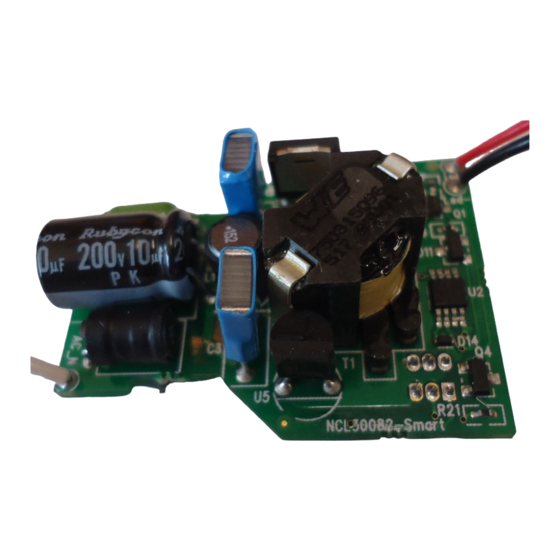
EVAL BOARD USER'S MANUAL
(Top View)
(Bottom View)
Figure 1. NCL30082SMRTGEVB
Evaluation Board
Publication Order Number:
EVBUM2307/D
Advertisement

Subscribe to Our Youtube Channel
Related Manuals for ON Semiconductor NCL30082SMRTGEVB


Summary of Contents for ON Semiconductor NCL30082SMRTGEVB
- Page 1 Start Up Time (from Enable On) < 1 ms EMI (Conducted) Class B FCC/CISPR (Bottom View) Key Features Figure 1. NCL30082SMRTGEVB • Single Mains Evaluation Board • Integrated Auto-Recovery Fault Protection (Can be Latched by Choice of Options) Over Temperature on Board (a PCB Mounted NTC) ♦...
-
Page 2: Theory Of Operation
NCL30082SMRTGEVB THEORY OF OPERATION Power Stage CrM Timing The power stage for the demo board is a non-isolated In the off time, the voltage on the transformer/inductor coupled SEPIC converter. The controller has a built in forward biases D and D9. When the current in the control algorithm that is specific to the flyback transfer magnetic has reached zero, the voltage collapses to zero. - Page 3 NCL30082SMRTGEVB Thermal Protection Programmable OVP There is an internal current source from the SD pin. While the SD pin has a current source for the OTP, it can Placing an NTC from the SD pin to ground will allow the be overcome raising the voltage on the SD pin.
- Page 4 NCL30082SMRTGEVB Interface Control Signals the power on startup time to be longer than 0.5 s since power on timing is now a one-time event. In this case, R START On/Off Control are optimized for low power consumption rather START1 The on/off control defaults to “on” if left open. Grounding than an optimized startup time.
- Page 5 NCL30082SMRTGEVB SCHEMATIC DAMP 180 W +HVDC AC_L FUSE 1.5 mH 10 mF 100 nF 200 V − 250 V 1.5 mH AC_N ABS10 Figure 3. Input Circuit MM5Z15VT1G 56 kW 4.7 mF 100 V MMBTA06LT1G NDD02N60Z Figure 4. Main Schematic...
- Page 6 NCL30082SMRTGEVB 3.32 kW Figure 5. Interface Schematic www.onsemi.com...
- Page 7 NCL30082SMRTGEVB GERBER VIEWS Figure 6. Top Side PCB Figure 7. Bottom Side PCB www.onsemi.com...
- Page 8 NCL30082SMRTGEVB Figure 8. PCB Outline www.onsemi.com...
- Page 9 NCL30082SMRTGEVB All Wire 6″ ±0.5″. Strip Ends 0.5″ Wire 3 Red Wire 1 White Wire 4 Black Place the Label on Top of T1 “NCL30082SMRTGEVB” “Rev( )” Wire 2 White L2 Mounts Horizontally Figure 9. Assembly Notes Top Bevel Edge of D4 Indicates Polarity J7 on the Solder Side Figure 10.
- Page 10 NCL30082SMRTGEVB CIRCUIT BARD FABRICATION NOTES 11. Size tolerance of plated holes: ±0.003″: non-plated 1. Fabricate per IPC−6011 and IPC6012. Inspect to IPA−A−600 Class 2 or updated standard. holes ±0.002″. 2. Printed Circuit Board is defined by files listed in 12. All holes shall be ±0.003″ of their true position fileset.
- Page 11 NCL30082SMRTGEVB SEPIC INDUCTOR SPECIFICATION Figure 11. SEPIC Inductor Specification www.onsemi.com...
- Page 12 NCL30082SMRTGEVB ECA PICTURES Figure 12. Top View Figure 13. Bottom View www.onsemi.com...
-
Page 13: Test Procedure
NCL30082SMRTGEVB TEST PROCEDURE Equipment Needed Test Connections • 1. Connect the LED load to the red(+) and black(−) AC Source – 90 to 135 V ac 50/60 Hz minimum 500 W leads through the ammeter shown in Figure 14. capability Caution: Observe the correct polarity or the load •... - Page 14 NCL30082SMRTGEVB TEST DATA Figure 15. Efficiency over Load Figure 16. Regulation over Line www.onsemi.com...
- Page 15 NCL30082SMRTGEVB Figure 17. Cross Regulation Effect of +3.3 Load on Output Current Figure 18. Cross Regulation Effect of Output Current on +3.3 V Output www.onsemi.com...
- Page 16 NCL30082SMRTGEVB Figure 19. Standby Power Consumption over Line Figure 20. Start Up with AC Applied 120 V Maximum Load Figure 21. Start Up with Enable www.onsemi.com...
-
Page 17: Bill Of Materials
NCL30082SMRTGEVB BILL OF MATERIALS Table 3. NCL30082SMRTGEVB BILL OF MATERIALS Substitution Qty. Reference Part Manufacturer Manufacturer Part Number PCB Footprint Allowed C13, C15, C 4.7 mF Taiyo Yuden EMK107ABJ475KA-T 4.7 mF, 100 V 12061Z475KAT2A 1206 C3, C5 100 nF, 250 V... - Page 18 onsemi, , and other names, marks, and brands are registered and/or common law trademarks of Semiconductor Components Industries, LLC dba “onsemi” or its affiliates and/or subsidiaries in the United States and/or other countries. onsemi owns the rights to a number of patents, trademarks, copyrights, trade secrets, and other intellectual property. A listing of onsemi’s product/patent coverage may be accessed at www.onsemi.com/site/pdf/Patent−Marking.pdf.
- Page 19 Mouser Electronics Authorized Distributor Click to View Pricing, Inventory, Delivery & Lifecycle Information: onsemi NCL30082SMRTGEVB...
Need help?
Do you have a question about the NCL30082SMRTGEVB and is the answer not in the manual?
Questions and answers