Advertisement
Quick Links
EVBUM2528/D
NCP51705 Mini Evaluation
Board User's Manual
NCP51705 SiC Driver Evaluation Board
for Existing or New PCB Designs
INTRODUCTION
Purpose
This document describes the use and applications for the
NCP51705 SiC driver mini EVB. The EVB is designed on
a four layer PCB and includes the NCP51705 driver and all
the necessary drive circuitry. The EVB also includes an
on−board digital isolator and the ability to solder any
MOSFET or SiC MOSFET in a T0247 high voltage
package. The EVB does not include a power stage and is
generic from the point of view that it is not dedicated to any
particular topology. It can be used in any low−side or
high−side power switching application. For bridge
configurations two or more of these EVBs can be configured
in a totem pole type drive configuration. The EVB can be
considered as an isolator+driver+T0247 discrete module.
NCP51705 Description
The NCP51705 driver is designed to primarily drive SiC
MOSFET transistors. To achieve the lowest possible
© Semiconductor Components Industries, LLC, 2017
April, 2019 − Rev. 1
EVAL BOARD USER'S MANUAL
conduction losses, the driver is capable of delivering the
maximum allowable gate voltage to the SiC MOSFET
device. By providing high peak current during turn−on and
turn−off, switching losses are also minimized. For improved
reliability, dV/dt immunity and even faster turn−off, the
NCP51705 can utilize its on−board charge pump to generate
a user selectable negative voltage rail.
For full compatibility and to minimize the complexity of
the bias solution in isolated gate drive applications the
NCP51705 also provides an externally accessible 5V rail to
power the secondary side of digital or high speed opto
isolators.
The NCP51705 offers important protection functions
such as under−voltage lockout monitoring for the bias power
and thermal shutdown based on the junction temperature of
the driver circuit.
1
www.onsemi.com
Publication Order Number:
EVBUM2528/D
Advertisement

Subscribe to Our Youtube Channel
Related Manuals for ON Semiconductor NCV51705


Summary of Contents for ON Semiconductor NCV51705
- Page 1 EVBUM2528/D NCP51705 Mini Evaluation Board User's Manual NCP51705 SiC Driver Evaluation Board for Existing or New PCB Designs www.onsemi.com INTRODUCTION EVAL BOARD USER’S MANUAL Purpose This document describes the use and applications for the conduction losses, the driver is capable of delivering the NCP51705 SiC driver mini EVB.
- Page 2 EVBUM2528/D NCP51705 Block Diagram SVDD 5V REG DESAT / 25 mA CURRENT 22 DESAT/CS SENSE UVSET UVLO 5V_OK VDD_OK PROTECTION LOGIC VEE_OK OUTSRC DRIVER INPUT LOGIC OUTSRC LOGIC IN− & LEVEL OUTSNK SHIFT OUTSNK CHARGE PUMP CPCLK 16 PGND SGND CHARGE PUMP POWER STAGE PGND...
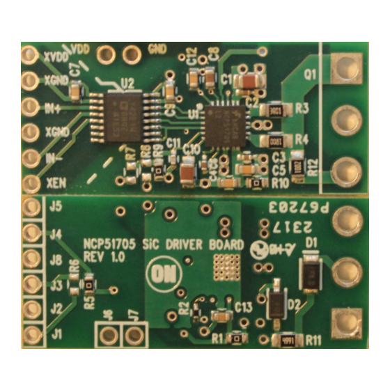
- Page 3 EVBUM2528/D SUMMARY OF EVB EVB Photos Figure 2. NCP51705 EVB (35 mm x 15 mm x 5 mm) − Top and Bottom View (T0−247 Shown for Scale) www.onsemi.com...
-
Page 4: Evb Schematic
EVBUM2528/D EVB Schematic Figure 3. NCP51705 EVB Schematic Table 1. BILL OF MATERIALS Item Reference Value Part Number Description Manufacturer Pkg Type C1 C10 2.2 mF CGA4J3X7R1H225M125AE CAP, SMD, CERAMIC, 50 V, C2 C13 100 nF C1005X7R1H104M050BE CAP, SMD, CERAMIC, 50 V, 47 nF GRM155R71E473KA88D CAP, SMD, CERAMIC, 25 V,... - Page 5 EVBUM2528/D Table 1. BILL OF MATERIALS Item Reference Value Part Number Description Manufacturer Pkg Type R1 R5 RC0603JR−070RL RES, SMD, 1/10 W R9−10 113k RC0402FR−07200KL RES, SMD, 1/16 W 3.01 RMCF0805FT3R01 RES, SMD, 1/8 W RMCF0805FT1R00 RES, SMD, 1/8 W R6−8 RES, SMD, 1/10 W 4.99k...
- Page 6 EVBUM2528/D Figure 5. Bottom Assembly Figure 6. Top Layer www.onsemi.com...
- Page 7 EVBUM2528/D Figure 7. Layer 2 Figure 8. Layer 3 Figure 9. Bottom Layer www.onsemi.com...
- Page 8 EVBUM2528/D I/O Connectors and “secondary” ground but there is 1.5 kV galvanic There are 7 I/O connectors described in Table 2 below. isolation across the isolation boundary. It is especially The mC (or, PWM control IC) output (J3, J4), the XVDD and important to maintain isolation in high−side, high−voltage, XGND (J1, J2) and the XEN (J5) signals are noted as switching applications where the “secondary”...
- Page 9 EVBUM2528/D EVB INSTALL CONFIGURATIONS Mounting into Existing PCB − Option 1 The NCP51705, SiC Driver Mini EVB can be mounted plated thru−holes and into the main PCB. Or, if necessary, into an existing power board, shown as “Main PCB” in the gate lead of the T0−247, SiC MOSFET can be soldered Figure 10.
- Page 10 EVBUM2528/D Option – Cut T0− 247 gate lead T0− 247 Mini EVB T0− 247 PWM Input T0− 247 T0− 247 (flying lead) Mini EVB Mini EVB Main PCB Main PCB Back View Side View Figure 11. Mini EVB Installation − Option 2 Recommended Procedure for Option 2 Mounting into an 9.
- Page 11 EVBUM2528/D T0− 247 T0− 247 80.0 (min) Mini EVB Mini EVB Main PCB Back View Side View Figure 12. New PCB Design using Shoulder Pins (80 mil minimum mounting height) T0− 247 T0− 247 80.0 (min) Mini EVB Mini EVB Main PCB Back View Side View...
- Page 12 EVBUM2528/D TESTING WITHOUT INSTALLING INTO A PCB The NCP51705, SiC Driver Mini EVB can also be tested from the 5 V DC bias (XVDD and XGND). The without installing into a main PCB. However, since this recommended series load of 470 pF and 4.99 W is close to EVB was designed for small form factor there are no test what might be representative of a SiC gate drive input points included for connecting voltage probes.
- Page 13 EVBUM2528/D UVSET internal DESAT threshold is fixed at V =7.5V and DESAT(TH) The UVSET function is set by R2 and determines the the DESAT signal amplitude is adjustable by R11. UVLO turn−on threshold. The EVB is preconfigured with R11 = 4.99 kW may not be the correct resistor value for R2 = 113 kW which equates to UVLO turn−on (V ) of some applications.
- Page 14 EVBUM2528/D WAVEFORMS Figure 16. IN+ = 150 kHz, 50%, VDESAT = 5 V, DESAT Inactive Figure 17. IN+ = 80 kHz, 50%, VDESAT = 7.5 V, DESAT Active www.onsemi.com...
- Page 15 EVBUM2528/D Figure 18. IN+ Falling to XEN Rising Delay, tD1 = 83 ns Figure 19. IN+ Rising to XEN Falling Delay, tD2 = 34 ns www.onsemi.com...
- Page 16 onsemi, , and other names, marks, and brands are registered and/or common law trademarks of Semiconductor Components Industries, LLC dba “onsemi” or its affiliates and/or subsidiaries in the United States and/or other countries. onsemi owns the rights to a number of patents, trademarks, copyrights, trade secrets, and other intellectual property. A listing of onsemi’s product/patent coverage may be accessed at www.onsemi.com/site/pdf/Patent−Marking.pdf.
Need help?
Do you have a question about the NCV51705 and is the answer not in the manual?
Questions and answers