Advertisement
Quick Links
www.ti.com
User's Guide
INA851 Evaluation Module
This user's guide contains information and support documentation for the INA851 evaluation module (EVM).
Included are the circuit description, jumper settings, required connections, printed circuit board (PCB) layout,
schematic, and bill of materials of the INA851EVM. Throughout this document, the terms evaluation board,
evaluation module, and EVM are synonymous with the INA851EVM.
SBOU273A – FEBRUARY 2022 – REVISED NOVEMBER 2022
Submit Document Feedback
ABSTRACT
Copyright © 2022 Texas Instruments Incorporated
INA851 Evaluation Module
1
Advertisement

Related Manuals for Texas Instruments INA851EVM


Summary of Contents for Texas Instruments INA851EVM
- Page 1 This user's guide contains information and support documentation for the INA851 evaluation module (EVM). Included are the circuit description, jumper settings, required connections, printed circuit board (PCB) layout, schematic, and bill of materials of the INA851EVM. Throughout this document, the terms evaluation board, evaluation module, and EVM are synonymous with the INA851EVM.
- Page 2 List of Tables Table 1-1. Related Documentation.............................. Table 3-1. Default Jumper Configuration............................. Table 4-1. INA851EVM Supply-Range Specifications......................... Table 5-1. INA851EVM Input and Output Connections....................... Table 7-1. INA851EVM Bill of Materials.............................15 Trademarks All trademarks are the property of their respective owners.
- Page 3 (ADCs) with fully differential inputs. A single external resistor sets any gain from 0.2 V/V to 10,000 V/V. The device features super-beta input transistors from Texas Instruments, which provide ultra-low input offset voltage, offset drift, input bias current, input voltage noise, and current noise.
- Page 4 (default), or to external voltages using connector J9. Revision A of the INA851EVM allows access to the FDA_IN– and FDA_IN+ pins with optional capacitors C7 and C18. These capacitors are in parallel with the INA851 output stage internal feedback resistors to implement noise filtering.
- Page 5 Jumper Settings 3 Jumper Settings Figure 3-1 details the default jumper settings of the INA851EVM. Table 3-1 explains the configuration for these jumpers. Figure 3-1. INA851EVM Default Jumper Settings Table 3-1. Default Jumper Configuration Jumper Function Default Position Description...
- Page 6 The positive power-supply connection is labeled +VCC, the negative power-supply connection is labeled –VEE, and the ground connection is labeled GND. To connect power to the INA851EVM, insert wires into each terminal of J1 and then tighten the screws to make the connection.
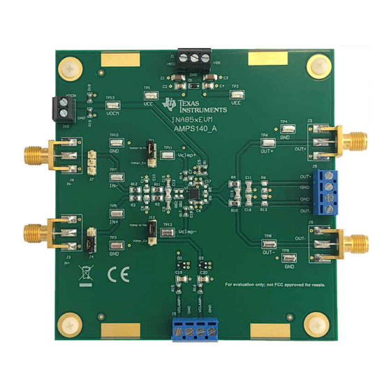
- Page 7 5 Input and Output Connections The instrumentation amplifier input signal connections for the INA851EVM are provided through the use of SMA connectors J3, J6, and test points TP5, TP7, located at the left of the EVM. The VOCM input is provided through screw-terminal connector J10, located on the left of the board.
- Page 8 Input and Output Connections www.ti.com Table 5-1 summarizes the input and output connectors and corresponding test points. Table 5-1. INA851EVM Input and Output Connections Connector Signal Comment Test Point Designator IN– OUT+ OUT– J5.4 OUT+ Screw terminal J5.3 Screw terminal J5.2...
- Page 9 0.2 V/V. In addition, the evaluation board provides footprints R3, R12, C10, C8, and C14 for optional input low-pass filters, and footprints for load resistors R6 and R13. These additional component footprints in the layout allow the user to customize the evaluation circuit. For a full schematic of the INA851EVM, Figure 7-1.
- Page 10 Schematic, PCB Layout, and Bill of Materials www.ti.com Figure 7-2. Top Overlay PCB Layout INA851 Evaluation Module SBOU273A – FEBRUARY 2022 – REVISED NOVEMBER 2022 Submit Document Feedback Copyright © 2022 Texas Instruments Incorporated...
- Page 11 Schematic, PCB Layout, and Bill of Materials Figure 7-3. Top Layer PCB Layout SBOU273A – FEBRUARY 2022 – REVISED NOVEMBER 2022 INA851 Evaluation Module Submit Document Feedback Copyright © 2022 Texas Instruments Incorporated...
- Page 12 Schematic, PCB Layout, and Bill of Materials www.ti.com Figure 7-4. Ground Layer PCB Layout INA851 Evaluation Module SBOU273A – FEBRUARY 2022 – REVISED NOVEMBER 2022 Submit Document Feedback Copyright © 2022 Texas Instruments Incorporated...
- Page 13 Schematic, PCB Layout, and Bill of Materials Figure 7-5. Power Layer PCB Layout SBOU273A – FEBRUARY 2022 – REVISED NOVEMBER 2022 INA851 Evaluation Module Submit Document Feedback Copyright © 2022 Texas Instruments Incorporated...
- Page 14 Schematic, PCB Layout, and Bill of Materials www.ti.com Figure 7-6. Bottom Layer PCB Layout INA851 Evaluation Module SBOU273A – FEBRUARY 2022 – REVISED NOVEMBER 2022 Submit Document Feedback Copyright © 2022 Texas Instruments Incorporated...
- Page 15 Schematic, PCB Layout, and Bill of Materials 7.3 Bill of Materials Table 7-1 lists the INA851EVM bill of materials (BOM). Table 7-1. INA851EVM Bill of Materials Designator Quantity Value Description Package Reference Part Number Manufacturer !PCB1 Printed Circuit Board...
- Page 16 Changed Figure 2-1, EVM Simplified Schematic, to show updated FDA_IN– and FDA_IN+ connections..• Changed Figure 3-1, INA851EVM Default Jumper Settings, to show updated RTM Revision A silkscreen..• Changed Figure 4-1, INA851EVM Voltage Supply Connections, to show FDA_IN– and FDA_IN+ pins...
- Page 17 STANDARD TERMS FOR EVALUATION MODULES Delivery: TI delivers TI evaluation boards, kits, or modules, including any accompanying demonstration software, components, and/or documentation which may be provided together or separately (collectively, an “EVM” or “EVMs”) to the User (“User”) in accordance with the terms set forth herein.
- Page 18 www.ti.com Regulatory Notices: 3.1 United States 3.1.1 Notice applicable to EVMs not FCC-Approved: FCC NOTICE: This kit is designed to allow product developers to evaluate electronic components, circuitry, or software associated with the kit to determine whether to incorporate such items in a finished product and software developers to write software applications for use with the end product.
- Page 19 www.ti.com Concernant les EVMs avec antennes détachables Conformément à la réglementation d'Industrie Canada, le présent émetteur radio peut fonctionner avec une antenne d'un type et d'un gain maximal (ou inférieur) approuvé pour l'émetteur par Industrie Canada. Dans le but de réduire les risques de brouillage radioélectrique à...
- Page 20 www.ti.com EVM Use Restrictions and Warnings: 4.1 EVMS ARE NOT FOR USE IN FUNCTIONAL SAFETY AND/OR SAFETY CRITICAL EVALUATIONS, INCLUDING BUT NOT LIMITED TO EVALUATIONS OF LIFE SUPPORT APPLICATIONS. 4.2 User must read and apply the user guide and other available documentation provided by TI regarding the EVM prior to handling or using the EVM, including without limitation any warning or restriction notices.
- Page 21 Notwithstanding the foregoing, any judgment may be enforced in any United States or foreign court, and TI may seek injunctive relief in any United States or foreign court. Mailing Address: Texas Instruments, Post Office Box 655303, Dallas, Texas 75265 Copyright © 2019, Texas Instruments Incorporated...
- Page 22 TI products. TI’s provision of these resources does not expand or otherwise alter TI’s applicable warranties or warranty disclaimers for TI products. TI objects to and rejects any additional or different terms you may have proposed. IMPORTANT NOTICE Mailing Address: Texas Instruments, Post Office Box 655303, Dallas, Texas 75265 Copyright © 2022, Texas Instruments Incorporated...
Need help?
Do you have a question about the INA851EVM and is the answer not in the manual?
Questions and answers