Table of Contents
Advertisement
Quick Links
ISL71040MEV1Z
Evaluation Board
The ISL71040MEV1Z evaluation platform is designed to evaluate the ISL71040M. The ISL71040M is designed to
drive enhancement mode Gallium Nitride (GaN) FETs in isolated topologies and boost type configurations. It
operates across a supply range of 4.5V to 13.2V and offers both non-inverting and inverting inputs to satisfy
non-inverting and inverting gates drive within a single device. The ISL71040M has a 4.5V gate drive voltage
(V
) that is generated using an internal regulator that prevents the gate voltage from exceeding the maximum
DRV
gate-to-source rating of enhancement mode GaN FETs. The gate drive voltage also features an Undervoltage
Lockout (UVLO) protection that ignores the inputs (IN/INB) and keeps OUTL turned on to ensure the GaN FET is
in an OFF state whenever VDRV is below the UVLO threshold. The ISL71040M inputs can withstand voltages up
to 14.7V regardless of the V
controllers. The split outputs of the ISL71040M offer the flexibility to adjust the turn-on and turn-off speed
independently by adding additional impedance to the turn-on/off paths.
Key Features
• Wide V
range single
DD
○ 4.5V to 13.2V
• Location provided for load resistors to switch the GaN FET with a load
• SMA connector on the gate drive voltage to analyze the gate waveforms
• Drain/source sense test points to analyze the drain to source waveforms
• Banana jack connectors for power supplies and drain/source connections
Specifications
• V
range: 4.5V to 13.2V
DD
Ordering Information
Part Number
ISL71040MEV1Z
Related Literature
For a full list of related documents, visit our website:
•
ISL71040M
device page
R12UZ0042EU0200 Rev.2.0
Feb.9.21
voltage. This allows the ISL71040M inputs to be connected directly to most PWM
DD
ISL71040MEV1Z evaluation board
User Manual
Description
Page 1
Copyright © 2019
Advertisement
Table of Contents

Related Manuals for Intersil ISL71040MEV1Z


Summary of Contents for Intersil ISL71040MEV1Z
- Page 1 ISL71040MEV1Z Evaluation Board The ISL71040MEV1Z evaluation platform is designed to evaluate the ISL71040M. The ISL71040M is designed to drive enhancement mode Gallium Nitride (GaN) FETs in isolated topologies and boost type configurations. It operates across a supply range of 4.5V to 13.2V and offers both non-inverting and inverting inputs to satisfy non-inverting and inverting gates drive within a single device.
-
Page 2: Functional Description
ISL71040MEV1Z 1. Functional Description Functional Description The ISL71040M is a single channel, high speed enhanced mode GaN FET low-side driver for isolated power supplies and Synchronous Rectifier (SR) applications. The inputs stage can handle inputs to the 14.7V independent of V and offers both inverting and non-inverting inputs. -
Page 3: Undervoltage Lockout
ISL71040MEV1Z 1. Functional Description Undervoltage Lockout The VDD pin accepts a recommended supply voltage range of 4.5V to 13.2V and is the input to the internal linear regulator. VDRV is the output of the regulator and is equal to 4.5V. VDRV provides the bias for all internal circuitry and the gate drive voltage for the output stage. - Page 4 ISL71040MEV1Z 1. Functional Description Driver Power Dissipation The ISL71040M power dissipation is dominated by the losses associated with the gate charge of the driven bridge FETs and the switching frequency. The internal bias current also contributes to the total dissipation but is usually not significant compared to the gate charge losses.
- Page 5 ISL71040MEV1Z 2. General PCB Layout Guidelines General PCB Layout Guidelines The AC performance of the ISL71040M depends significantly on the design of the Printed Circuit Board (PCB). The following layout design guidelines are recommended to achieve optimum performance: • Place the driver as close as possible to the driven power FET.
- Page 6 Drain Double Up On Several Layers as per Current Needs VDRV OUTH ISL71040M OUTL ISL73023SEH VSSP Source Double Up On Several Layers as per Current Needs Figure 1. PCB Layout Recommendation...
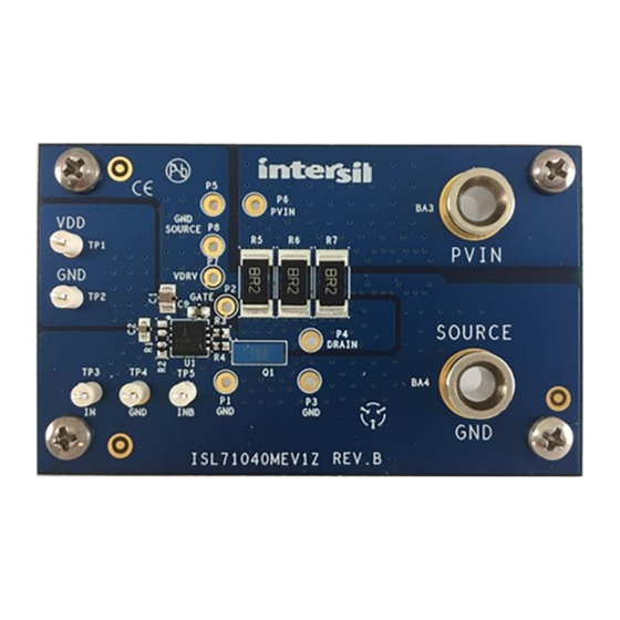
- Page 7 ISL71040MEV1Z 2. General PCB Layout Guidelines ISL71040MEV1Z Evaluation Board Figure 2. ISL71040MEV1Z Evaluation Board, Top View Figure 3. ISL71040MEV1Z Evaluation Board, Bottom View R12UZ0042EU0200 Rev.2.0 Page 7 Feb.9.21...
- Page 8 ISL71040MEV1Z Schematic Diagram PVIN 575-4 ISL73023SEH DRAIN 575-4 SOURCE VDRV VDRV GATE OUTH OUTH OUTL OUTL VSSP EPAD ISL71040MRTZ Figure 4. ISL71040MEV1Z Schematic...
-
Page 9: Bill Of Materials
ISL71040MEV1Z 2. General PCB Layout Guidelines Bill of Materials Table 2. Components Parts List Reference Designator Description Manufacturer Part Number R5, R6, R7 Surface Mount Power Resistor TE Connectivity 35228R2JT TP1, TP2, TP3, TP4, Miniature White Test Point 100 Pad 0.040 Thole... - Page 10 ISL71040MEV1Z 2. General PCB Layout Guidelines Figure 6. Bottom Silkscreen Figure 7. Top Layer R12UZ0042EU0200 Rev.2.0 Page 10 Feb.9.21...
- Page 11 ISL71040MEV1Z 2. General PCB Layout Guidelines Figure 8. Second Layer Figure 9. Third Layer R12UZ0042EU0200 Rev.2.0 Page 11 Feb.9.21...
- Page 12 ISL71040MEV1Z 2. General PCB Layout Guidelines Figure 10. Bottom Layer R12UZ0042EU0200 Rev.2.0 Page 12 Feb.9.21...
-
Page 13: Typical Performance Curves
ISL71040MEV1Z 3. Typical Performance Curves Typical Performance Curves Input 2V/Div DOFF 42.8ns 43.8ns : 9.4ns RISE : 7.6ns OUTH/L FALL 125°C 25°C -55°C Figure 12. Input Propagation Delay Figure 11. V Short-Circuit Current vs Temperature Input 2V/Div DOFF 44.0ns 46.7ns OUTH/L : 9.1ns... -
Page 14: Revision History
ISL71040MEV1Z 4. Revision History Revision History Rev. Date Description Feb.9.21 Updated BOM, schematic, layout files, and photos to reflect Rev B build. Feb.21.19 Initial release R12UZ0042EU0200 Rev.2.0 Page 14 Feb.9.21... -
Page 15: Corporate Headquarters
IMPORTANT NOTICE AND DISCLAIMER RENESAS ELECTRONICS CORPORATION AND ITS SUBSIDIARIES (“RENESAS”) PROVIDES TECHNICAL SPECIFICATIONS AND RELIABILITY DATA (INCLUDING DATASHEETS), DESIGN RESOURCES (INCLUDING REFERENCE DESIGNS), APPLICATION OR OTHER DESIGN ADVICE, WEB TOOLS, SAFETY INFORMATION, AND OTHER RESOURCES “AS IS” AND WITH ALL FAULTS, AND DISCLAIMS ALL WARRANTIES, EXPRESS OR IMPLIED, INCLUDING, WITHOUT LIMITATION, ANY IMPLIED WARRANTIES OF MERCHANTABILITY, FITNESS FOR A PARTICULAR PURPOSE, OR NON-INFRINGEMENT OF THIRD PARTY INTELLECTUAL PROPERTY RIGHTS.
Need help?
Do you have a question about the ISL71040MEV1Z and is the answer not in the manual?
Questions and answers