Table of Contents
Advertisement
Quick Links
ISL73033SLHEV1Z
Evaluation Board
The ISL73033SLHEV1Z evaluation board evaluates the performance of the ISL73033SLH. The ISL73033SLH is
a radiation hardened Driver-GaN Power Stage that integrates a 4.5V gate driver and a 100V, 7.5mΩ
enhancement-mode Gallium Nitrade FET (eGaN FET) in a single 8mmx8mm BGA package. The device simplifies
the Printed Circuit Board (PCB) layout by integrating a driver plus GaN FET in one package and is designed for
boost and isolated DC/DC converter topologies. The driver operates with a supply voltage from 4.5V to 13.2V and
has both inverting (INB) and non-inverting (IN) inputs to satisfy requirements for inverting and non-inverting logic
drives with a single device.
The ISL73003SLHEV1Z evaluation board is configured as a common-source open drain 100V current sense load
switch with three on board 2512 sized 220mΩ resistors in parallel (73.3mΩ).
Specifications
▪ Gate Driver Supply Voltage Range: 4.5V to 13.2V
▪ GaN FET Drain-to-Source Voltage: 100V (80V
▪ Recommended Operating Frequency: Up to 5MHz (limited by Drain-Source rise and fall times)
▪ Board Dimension: 4cm x 4.5cm
▪ Board Layers: 4
▪ Board PCB Copper Weight: 2oz outer; 1oz inner
▪ Board Revision: A
Ordering Information
Part Number
ISL73033SLHEV1Z
Related Literature
For a full list of related documents, visit our website:
▪
ISL73033SLH
device page
VDD
VDRV
ISL73033SLH
IN
X0116715 Rev.1.0
Jan.12.21
maximum recommended operation)
DC
ISL73033SLH evaluation board
DRAIN
SOURCE
Figure 1. ISL73033SLHEV1Z Block Diagram
User Manual
Description
GND
PVIN
Page 1
Advertisement
Table of Contents

Related Manuals for Intersil ISL73033SLHEV1Z


Summary of Contents for Intersil ISL73033SLHEV1Z
- Page 1 ISL73033SLHEV1Z Evaluation Board The ISL73033SLHEV1Z evaluation board evaluates the performance of the ISL73033SLH. The ISL73033SLH is a radiation hardened Driver-GaN Power Stage that integrates a 4.5V gate driver and a 100V, 7.5mΩ enhancement-mode Gallium Nitrade FET (eGaN FET) in a single 8mmx8mm BGA package. The device simplifies the Printed Circuit Board (PCB) layout by integrating a driver plus GaN FET in one package and is designed for boost and isolated DC/DC converter topologies.
-
Page 2: Table Of Contents
ISL73033SLHEV1Z PCB Guidelines ........ -
Page 3: Functional Description
ISL73033SLHEV1Z User Manual 1. Functional Description The ISL73033SLHEV1Z evaluation board evaluates the performance of the ISL73033SLH. The driver operates with a supply voltage from 4.5V to 13.2V and has both inverting (INB) and non-inverting (IN) inputs to satisfy requirements for inverting and non-inverting logic drives with a single device. -
Page 4: Isl73033Slhev1Z Pcb Guidelines
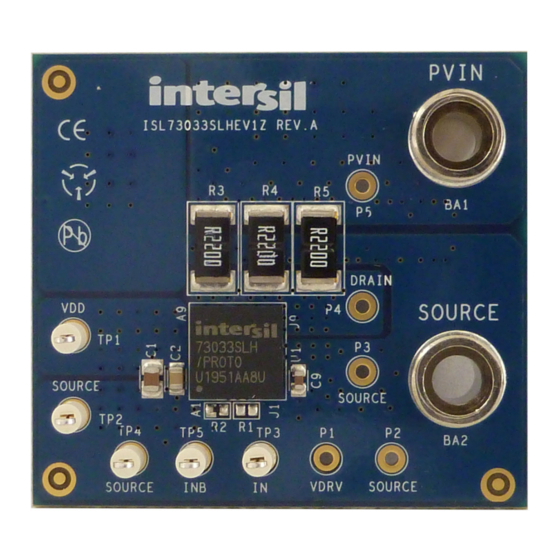
Renesas also recommends using a conductively filled via underneath the balls to additional PCB layers to help carry heat away from the package. Evaluation Board Figure 2. ISL73033SLHEV1Z Evaluation Board (Top) Figure 3. ISL73033SLHEV1Z Evaluation Board (Bottom) X0116715 Rev.1.0 Page 4 Jan.12.21... -
Page 5: Circuit Schematic
Circuit Schematic VDRV PVIN VDDP VDD MUST BE SHORTED TO VDDP DRAIN VDRV VDRV DRAIN DRAIN ISL73033SEHM/PROTO SOURCE SOURCE SOURCE VSS MUST BE SHORTED TO VSSP VSSP Figure 4. ISL73033SLHEV1Z Circuit Schematic... -
Page 6: Bill Of Materials
ISL73033SLHEV1Z User Manual Bill of Materials Reference Designator Description Manufacturer Manufacturer Part PWB-PCB, ISL73033SLHEV1Z, Imagineering Inc ISL73033SLHEV1ZREVAPCB REVA, ROHS CAP-AEC-Q200, SMD, 0805, CGA4J1X7R1E475K125AC 4.7µF, 25V, 10%, X7R, ROHS C3, C4, C5, C6, C7, C8 CAP, SMD, 1210, 0.22µF, 250V, Murata... -
Page 7: Board Layout
ISL73033SLHEV1Z User Manual Board Layout Figure 5. Silkscreen Top Figure 6. Top Layer Figure 7. Layer 2 Figure 8. Layer 3 Figure 9. Bottom Layer Figure 10. Silkscreen Bottom X0116715 Rev.1.0 Page 7 Jan.12.21... -
Page 8: Typical Performance
ISL73033SLHEV1Z User Manual 3. Typical Performance DRAIN 100Ω VDD = 10V DRAIN VDRV ISL73033SLH SOURCE Figure 11. Waveform 1 Figure 12. Test Circuit for Waveform 1 DRAIN VDRV 8.2Ω IDS 2.4A/div 150µF 100V VDD = 10V DRAIN VDRV ISL73033SLH SOURCE Figure 13. -
Page 9: Revision History
ISL73033SLHEV1Z User Manual 4. Revision History Rev. Description Description Jan.12.21 Initial release X0116715 Rev.1.0 Page 9 Jan.12.21... - Page 10 IMPORTANT NOTICE AND DISCLAIMER RENESAS ELECTRONICS CORPORATION AND ITS SUBSIDIARIES (“RENESAS”) PROVIDES TECHNICAL SPECIFICATIONS AND RELIABILITY DATA (INCLUDING DATASHEETS), DESIGN RESOURCES (INCLUDING REFERENCE DESIGNS), APPLICATION OR OTHER DESIGN ADVICE, WEB TOOLS, SAFETY INFORMATION, AND OTHER RESOURCES “AS IS” AND WITH ALL FAULTS, AND DISCLAIMS ALL WARRANTIES, EXPRESS OR IMPLIED, INCLUDING, WITHOUT LIMITATION, ANY IMPLIED WARRANTIES OF MERCHANTABILITY, FITNESS FOR A PARTICULAR PURPOSE, OR NON-INFRINGEMENT OF THIRD PARTY INTELLECTUAL PROPERTY RIGHTS.
Need help?
Do you have a question about the ISL73033SLHEV1Z and is the answer not in the manual?
Questions and answers