Table of Contents
Advertisement
Quick Links
・This document is a reference specification.
・SHARP reserves the right to make changes in the
contents described herein at any time without
notice in order to improve design or reliability.
・Regarding final design, please order delivery
specification from SHARP.
©Copyright 2017 SHARP All rights reserved
DEVICE SPECIFICATION
LCD Module
LS013B7DH01
MODEL No.
These parts are complied with the RoHS directive.
FOR
DEVEROPMENT DEPARTMENT
BU Ⅰ BUSINESS UNIT Ⅳ
DISPLAY DEVICE COMPANY
SHARP CORPORATION
No.
LD-29608A
DATE
13-Jun-17
-
REV.
Advertisement
Table of Contents

Related Manuals for Sharp LS013B7DH01


Summary of Contents for Sharp LS013B7DH01
- Page 1 MODEL No. These parts are complied with the RoHS directive. ・This document is a reference specification. ・SHARP reserves the right to make changes in the contents described herein at any time without notice in order to improve design or reliability.
- Page 2 改訂履歴 RECORDS OF REVISION Model No : LS013B7DH01 DATE REV No SUMMARY NOTE SPEC No. PAGE LCP-2111015 2011/3/29 First issue LCP- 2015/3/18 Change of Department in charge 2111015B Table 7-1 : Add MIN/MAX of "Panle Chromaticity" Figure 7-2 : Add Light source Type of...
- Page 3 ・Aerospace equipment ・Military and space applications ・Nuclear power control equipment ・Medical equipment for life support ・Trunk line commucation equipment h) Contact and consult with a SHARP representative in advance, if there are any questions about the contents of this publication. ©Copyright 2017 SHARP All rights reserved...
- Page 4 (6) Be careful to handle this LCD panel in order to avoid injury yourself as this panel is made of glass and have sharp edge. When the panel is broken, do not touch the glass. Although the panel is difficult to be scattered, touching the broken part may hurt your hands.
- Page 5 MODEL No. PAGE LD-29608A LS013B7DH01 【Set-Design Precautions】 (1) Disassembly of the LCD panel in any way voids the warranty and may permanently damage the LCD panel. (2) Do not expose the side of LCD panel and gate driver, etc. on the panel (circuit area outside panel display area) to light as it may not operate properly.
- Page 6 MODEL No. PAGE LD-29608A LS013B7DH01 (15) To prevent reduction in optical quality and abnormal display, avoid exposure and contamination of the LCD panel from epoxy resin (mine system curing agent) that comes out from the material and the packaging material used for the set side, the silicon adhesive (dealcoholization system and oxime system), and the tray blowing agents ( azo-compound), etc.
- Page 7 SPEC No. MODEL No. PAGE LD-29608A LS013B7DH01 【Operation Precautions】 (1) Do not use polychloroprene (CR) with LCD module. It will generate chlorine gas, which will damage the reliability of the connection part on LCD panel. (2) Be sure to use LCD module within the recommended operating conditions. Operating module out of the recommended range is not guaranteed even if it is in the absolute maximum rating.
- Page 8 SPEC No. MODEL No. PAGE LD-29608A LS013B7DH01 [Precautions for Storage] (1) After opening the package, do not leave the LCD panel in direct sun or under strong ultraviolet ray. Store in the dark place. (2) In temperature lower than specified rating, liquid crystal material will coagulate. In temperature higher than specified rating, it will liquefies.
- Page 9 SPEC No. MODEL No. PAGE LD-29608A LS013B7DH01 [Other Notice] (1) Operation outside specified environmental conditions cannot be guaranteed. (2) As power supply (VDD-GND、VDDA-GND) impedance is lowered during use, bus controller should be inserted near LCD module as much as possible.
-
Page 10: Table Of Contents
SPEC No. MODEL No. PAGE LD-29608A LS013B7DH01 Contents Page 1. Applocable Memory liquid crystal display ......................9 2. Characteristics ................................9 3. Mechanical Specification ............................9 4. Input terminal names and functions ........................10 5. Absolute Maximum Rating ............................. 13 6. -
Page 11: Applocable Memory Liquid Crystal Display
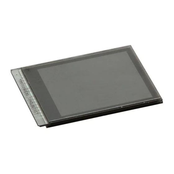
SPEC No. MODEL No. PAGE LD-29608A LS013B7DH01 1. Applocable Memory liquid crystal display This TFT-LCD module is a reflective active-matrix memory liquid crystal display module with CG silicone thin film transistor. Module outline is indicated in Figure 8-2 . Characteristics ・... -
Page 12: Input Terminal Names And Functions
SPEC No. MODEL No. PAGE LD-29608A LS013B7DH01 4. Input terminal names and functions Table4-1 Pin description Terminal Symbol I/O Function Remark Configurations - - 【Note 4-3】 TEST2 No connection 【Note 4-3】 TEST1 - - No connection SCLK INPUT NoPull Serial clock signal... - Page 13 SPEC No. MODEL No. PAGE LD-29608A LS013B7DH01 4-1) Input Signal States Table4-2 Input Signal States (Update & Symbol Voltage Boot Standby note Hold mode) EXTMODE=Hi SCLK Input 0 / 3V Hi / Lo Hi / Lo EXTMODE=Lo ※1 EXTMODE=Hi Input...
- Page 14 SPEC No. MODEL No. PAGE LD-29608A LS013B7DH01 4-2) Recommended Circuit < EXTMODE=“Lo” > < EXTMODE=“Hi” > COM Signal Serial Flag Input External COM Signal Input Open Open TEST1 TEST1 Open Open TEST2 TEST2 SCLK SCLK EXTCOMIN EXTCOMIN DISP DISP VDDA...
-
Page 15: Absolute Maximum Rating
SPEC No. MODEL No. PAGE LD-29608A LS013B7DH01 5. Absolute Maximum Rating Table5-1 Absolute Maximum Rating ( GND=0V ) Item Symbol Unit Remark Power Analog VDDA -0.3 +5.8 supply [Note 5-1] Logic -0.3 +5.8 voltage Input signal voltage(high) [Note 5-2] -... -
Page 16: Electrical Characteristics
SPEC No. MODEL No. PAGE LD-29608A LS013B7DH01 6. Electrical characteristics 6-1) TFT LCD panel drive Table6-1 Recommended operating Condition VSS(GND)=0V、Ta=+25℃ Item Symbol Min. Typ. Max. Unit Remark Analog VDDA +4.8 +5.0 +5.5 [Note 6-1-3] Power supply Voltage [Note 6-1-1] Logic +4.8... - Page 17 SPEC No. MODEL No. PAGE LD-29608A LS013B7DH01 6-2) Power supply sequence 6-2-1)Panel Power-ON Sequence EXTMODE (Hi or Lo) same time VDDA ※3 2clk ≦ T1 ※2 SCLK 0x00 0x20 30μs ≦ TA DISP ※1 ※1 30μs ≦ T4 30μs ≦ T3...
- Page 18 SPEC No. MODEL No. PAGE LD-29608A LS013B7DH01 ※Refer to timing chart and AC timing characteristics for detail ※1 TA and T3 may be opposite (however, TCOM polarity inversion will not occur even with EXTCOMIN between DISP=“Lo”.) Also, when DISP and EXTCOMIN are simultaneously started up, allow 30us or more before SCS starts up (It may be less than 60us).
- Page 19 SPEC No. MODEL No. PAGE LD-29608A LS013B7DH01 6-2-2)Panel Power-OFF Sequence EXTMODE (Hi or Lo) VDDA T7 ≧1clk ※2 SCLK 0x20 0x00 30μs ≦ T6 DISP ( EXTMODE=Hi ) EXTCO MIN ( EXTMODE=Lo ) Operating state ON ( Normal Operation ) Power-off Sequence TS : Off control...
- Page 20 SPEC No. MODEL No. PAGE LD-29608A LS013B7DH01 6-3) Input signal characteristics Table6-3-1 Recommend Operating Cunditions and DC Characteristics VDDA=+5.0V、VDD=+5.0V、GND=0V、Ta=25℃ Item Symbol Unit Remark When EXTMODE=Lo 【Note 6-3-1】 Frame frequency fSCS When EXTMODE=Hi 【Note 6-3-1】 Clock frequency fSCLK Vertical Interval 16.66...
- Page 21 SPEC No. MODEL No. PAGE LD-29608A LS013B7DH01 [Note 6-3-2] Please make the EXTCOMIN frequency less than the frame rate frequency. SCS EXTCOMIN Figure 6-3-1 EXTCOMIN Signal 1 [Note 6-3-3] When the display is maintained after writing of the displayed data, is not applied.
- Page 22 SPEC No. MODEL No. PAGE LD-29608A LS013B7DH01 6-4) Signal Timing ※SCS,SI,SCLK、DISP、EXTCOMIN: 3V input voltage twh SCS twl SCS tr SCS ts SCS th SCS tf SI tr SI tf SCS ts SI th SI twl SCLK twh SCLK SCLK tr SCLK...
- Page 23 SPEC No. MODEL No. PAGE LD-29608A LS013B7DH01 6-5) Power consumption Table6-5-1 Current Consumption Ta=25℃,SCS SCLK,Si,DISP,EXTCOMIN=+3V , VDD=+5V, VDDA=+5V Operating Mode Power consumption unit Remark Condition 1 Hold mode (no display data update) - μ W [Note 6-5-1] Display pattern : Vertical stripe display...
- Page 24 SPEC No. MODEL No. PAGE LD-29608A LS013B7DH01 6-6) Input Signal Timing Chart 6-6-1 Data update mode (1 line) Updates data of only one specified line. (M0=”Hi”、M2=”Lo”) DMY (don’t care) M2 DMY DMY DMY DMY AG0 AG1 AG2 AG3 AG4 AG5 AG6...
- Page 25 SPEC No. MODEL No. PAGE LD-29608A LS013B7DH01 6-6-2 Data Update Mode (Multiple Lines) Updates arbitrary multiple lines data. (M0= “Hi”、M2=“Lo”) DMY (don’t care) AG0 AG1 AG2 M2 DMY DMY DMY DMY AG0 AG1 AG2 AG3 AG4 AG5 AG6 D141 D142...
- Page 26 SPEC No. MODEL No. PAGE LD-29608A LS013B7DH01 ※ Data write period Data is being stored in 1 latch block of binary driver on panel. ※ Data transfer period For example, during GL2nd line data transfer period, GL 2 line address is latched and GL1st line data is transferred from 1 latch to pixel internal memory circuit at the same time.
- Page 27 SPEC No. MODEL No. PAGE LD-29608A LS013B7DH01 6-6-4 All Clear Mode Clears memory internal data and writes white. (M0=“Lo”、M2=“Hi”) Dummy Data (don’t care) SCLK Mode selection Data transfer period period ( More than 13clk ) ( 3ck ) Figure 6-6-4 All Clear mode M0: Mode flag.
- Page 28 SPEC No. MODEL No. PAGE LD-29608A LS013B7DH01 6-6-5 COM Inversion There are two types of inputs,COM signal serial input (EXTMODE=“Lo”) and external COM signal input (EXTMODE=“Hi”). EXTMODE=“Lo” ※1 ※1 ※1 (Internal Signal) ※2 ※2 Figure 6-6-5 COM Inversion (EXTMODE=Lo) M1:LC polarity inversion flag: If M1 is “Hi”...
- Page 29 SPEC No. MODEL No. PAGE LD-29608A LS013B7DH01 EXTMODE="Hi" (COM inversion timing has two conditions ) EXTCOMIN input during high period of the SCS signal ① ※2 EXTCOMIN ※1 ※1 ※1 ※1 (Internal Signal) Figure 6-6-6 COM Inversion 1 (EXTMODE=Hi) ※1 : COM inversion has been set by the falling edge of SCS signal (*not* toggle EXTCOMIN more than once while SCS is high) ※2 : The period of EXTCOMIN should be constant.
- Page 30 SPEC No. MODEL No. PAGE LD-29608A LS013B7DH01 6-7) Input Signal and Display, Gate address(Line) Setting <Data position in display[H,V]> LS013B7DH01 Serial No.*** P144 Display Side up P144 L167 P143 P144 L168 L168 L168 P*: Pixels position L*:Gate address line Figure 6-7-1 Data position...
- Page 31 SPEC No. MODEL No. PAGE LD-29608A LS013B7DH01 GL: Gate address line Table 6-4-1 Gate line address setting AG0 AG1 AG2 AG3 AG4 AG5 AG6 AG7 AG0 AG1 AG2 AG3 AG4 AG5 AG6 AG7 AG0 AG1 AG2 AG3 AG4 AG5 AG6 AG7...
-
Page 32: Optical Specification
SPEC No. MODEL No. PAGE LD-29608A LS013B7DH01 7. Optical specification Table 7-1 Optical specification VDD=VDDA=5V,Ta=25℃ Item Symbol Min. Typ. Max. unit Remark Θ21 - °(degree) Horizontal Viewing angle Θ22 - range [Note 7-1] Θ11 - CR≧2 °(degree) Vertical Θ12 -... - Page 33 MODEL No. PAGE LD-29608A LS013B7DH01 [Note 7-3] Optical characteristics measurement equipment. Figure 7-2 is for contrast ratio, reflectivity ratio, and panel chromaticity measurement, and Figure 7-3 is for response time measurement. Both are to be conducted in a dark room.
-
Page 34: Pin Assignment
SPEC No. MODEL No. PAGE LD-29608A LS013B7DH01 8. Pin Assignment 8-1) Pin Assignment of the 1.26” panel (Zebra connector) Figure 8-1 Pin Assignment 8-2) Outline dimension of the 1.26” (144 x 168) panel Figure 8-2 Outline dimension ©Copyright 2017 SHARP All rights reserved... - Page 35 SPEC No. MODEL No. PAGE LD-29608A LS013B7DH01 Zebra connector 8-3) Contact Resistance :lower than 100Ω 【Recommended zebra connector】 Shin-Etsu Polymer: SX type Recommended size L:27.7±0.2mm W:1.5±0.1mm H:2.0±0.1mm P:0.03mm Recommended compression ratio:15±8% The zebra connector placement position 1.SX Specifications(A figure of reference)...
-
Page 36: Display Qualities
SPEC No. MODEL No. PAGE LD-29608A LS013B7DH01 9. Display Qualities Please refer to the Incoming Inspection Standard (IIS). 10. External capacitors TEST1 TEST2 SCLK EXTCOMIN DISP VDDA EXTMODE VSSA TEST3 TEST4 Figure 10-1 External capacitor recommendation capacity value <Recommended capacity value>... -
Page 37: Marking
11-1) Displayed by printing. (Ink-jet print) The display position is shown in Figure. 11-1 Outline dimension diagram. Print location Print structure LS013B7DH01* 2X16Q00001A Model number Serial number specifications A:a single figure of the year (2 is 2012, 3 is 2013) B:month(1,2..9,X,Y,Z) -
Page 38: Packaging Form
SPEC No. MODEL No. PAGE LD-29608A LS013B7DH01 12.Packaging form 12-1) Carton storage condition 1) Piling number of cartons. : 10 (max) 2) Package quantity in one carton : 1,000 pcs 3) Carton size (Typ.) : 578 mm x 382 mm x 153 mm 4) Carton store environment: ・Temperature:... - Page 39 SPEC No. MODEL No. PAGE LD-29608A LS013B7DH01 12-2) Packaging form figure The packing condition is shown in Figure. 12-1 The packaging is designed such that the module does not break during transit. Figure. 12-1 Packaging Form ©Copyright 2017 SHARP All rights reserved...
-
Page 40: Reliability Test Conditions
SPEC No. MODEL No. PAGE LD-29608A LS013B7DH01 13.Reliability Test Conditions 13-1) Reliability Test Items Table13-1 ReliabilityTest Items Test Item Condition Remark Ta=80℃ 240h High temperature storage test (Non operating test) Ta=-30℃ 240h Low temperature storage test (Non operating test) Tp=40℃/95%RH...
Need help?
Do you have a question about the LS013B7DH01 and is the answer not in the manual?
Questions and answers