Table of Contents
Advertisement
Quick Links
One Technology Way • P.O. Box 9106 • Norwood, MA 02062-9106, U.S.A. • Tel: 781.329.4700 • Fax: 781.461.3113 • www.analog.com
Evaluating the
FEATURES
Supply voltages
Dual-supply: ±5 V to ±22 V
Single-supply: 8 V to 44 V
Protected against overvoltage on the device source pins
(S and SFB) on Terminal J2
Protected against signal voltages up to ±60 V
LEDs for visual overvoltage indication
Parallel interface compatible with 1.8 V logic
On-board LDO regulator for digital supply and control,
if required
EVALUATION KIT CONTENTS
EVAL-ADG5401FEBZ
DOCUMENTS NEEDED
ADG5401F
data sheet
EQUIPMENT NEEDED
DC voltage source
±5 V to ±22 V for dual supply
8 V to 44 V for single supply
Optional digital voltage source: 1.8 V to 5 V
Analog signal source (signal generator)
PLEASE SEE THE LAST PAGE FOR AN IMPORTANT
WARNING AND LEGAL TERMS AND CONDITIONS.
ADG5401F
Fault Protection, 6 Ω R
with 0.6 kΩ Feedback Channel
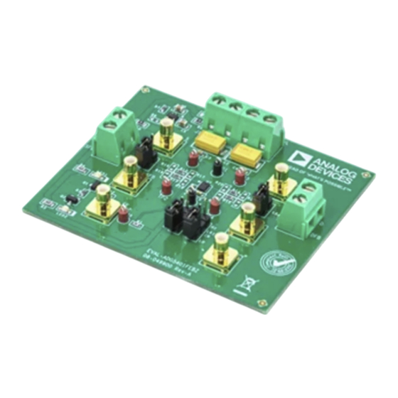
EVALUATION BOARD CONNECTION DIAGRAM
SIGNAL GENERATOR
Figure 1.
Rev. A | Page 1 of 8
EVAL-ADG5401FEBZ
ON
GENERAL DESCRIPTION
The EVAL-ADG5401FEBZ evaluation board for the
features one SPST switch channel and one feedback switch
channel. The
ADG5401F
and protection circuitry on the source pins (S and SFB) on
Terminal J2 and is protected against signals up to ±60 V in the
powered state and unpowered state.
Figure 1 shows the EVAL-ADG5401FEBZ in a typical evaluation
setup. The
ADG5401F
is soldered to the center of the EVAL-
ADG5401FEBZ, and two wire screw terminals (J2 and J3) are
provided to connect to each device source pin (S and SFB) and
drain pin (D and DFB). The J1 screw terminal powers the device
through three EVAL-ADG5401FEBZ supply pins (VDD, GND
and VSS), and a fourth pin (EXT_VL) provides a user defined
digital voltage of 1.8 V to 5 V, if required. Alternatively, a low
dropout (LDO) regulator (ADP7142) is provided for 5 V digital
voltage control and to supply both light emitting diodes (LEDs)
LED1 and LED2, which are mounted to provide visual
indication of the fault status of the switch.
For full specifications on the ADG5401F, see the
data sheet, which must be consulted in conjunction with this
user guide when using the EVAL-ADG5401FEBZ.
POWER SUPPLY
User Guide
UG-1755
, SPST Switch
ADG5401F
SPST switch has overvoltage detection
ADG5401F
Advertisement
Table of Contents

Related Manuals for Analog Devices EVAL-ADG5401FEBZ


Summary of Contents for Analog Devices EVAL-ADG5401FEBZ
-
Page 1: Features
Terminal J2 and is protected against signals up to ±60 V in the Protected against signal voltages up to ±60 V powered state and unpowered state. LEDs for visual overvoltage indication Figure 1 shows the EVAL-ADG5401FEBZ in a typical evaluation Parallel interface compatible with 1.8 V logic setup. The ADG5401F... -
Page 2: Table Of Contents
UG-1755 EVAL-ADG5401FEBZ User Guide TABLE OF CONTENTS Features ....................1 Power Supply .................4 Evaluation Kit Contents ..............1 Input Signals ..................4 Documents Needed ................1 Output Signals ................4 Equipment Needed ................1 Jumper Settings ..................5... -
Page 3: Getting Started
User Guide UG-1755 GETTING STARTED EVALUATION BOARD SETUP PROCEDURE To set up the EVAL-ADG5401FEBZ to perform a functionality test, take the following steps: The EVAL-ADG5401FEBZ operates independently and does Connect a power supply to the J1 connector. If a single supply... -
Page 4: Evaluation Board Hardware
GND and VSS terminals together and of the switch channel. The switch operation can be manually power the EVAL-ADG5401FEBZ with a supply from 8 V to 44 V. controlled using the headers on the LK1 link header. Or, remove... -
Page 5: Jumper Settings
The LK3 and LK4 link headers short both the S and SFB nodes Inserted 1 kΩ pull-up resistor at the FF pin and the D and DFB nodes on the EVAL-ADG5401FEBZ. When Removed No external pull-up resistor at the FF pin... -
Page 6: Evaluation Board Schematics And Artwork
UG-1755 EVAL-ADG5401FEBZ User Guide EVALUATION BOARD SCHEMATICS AND ARTWORK 0.1µF 0Ω 0Ω V DD ADG5401F 0Ω 0Ω 0.1µF Figure 3. EVAL-ADG5401FEBZ Schematic, Page 1 ADP7142AUJZ-5.0 VOUT 0Ω 0Ω SENSE/ADJ 10µF 0.1µF 4.7µF 0Ω 4.7µF 0Ω EXT_VL 10µF 0.1µF 0Ω 0Ω... - Page 7 EVAL-ADG5401FEBZ User Guide UG-1755 Figure 8. EVAL-ADG5401FEBZ, Layer 3 Figure 5. EVAL-ADG5401FEBZ, Silkscreen Figure 9. EVAL-ADG5401FEBZ, Bottom Layer Figure 6. EVAL-ADG5401FEBZ, Top Layer Figure 7. EVAL-ADG5401FEBZ, Layer 2 Rev. A | Page 7 of 8...
-
Page 8: Changes To Table 2
By using the evaluation board discussed herein (together with any tools, components documentation or support materials, the “Evaluation Board”), you are agreeing to be bound by the terms and conditions set forth below (“Agreement”) unless you have purchased the Evaluation Board, in which case the Analog Devices Standard Terms and Conditions of Sale shall govern. Do not use the Evaluation Board until you have read and agreed to the Agreement.
Need help?
Do you have a question about the EVAL-ADG5401FEBZ and is the answer not in the manual?
Questions and answers