Table of Contents
Advertisement
Quick Links
One Technology Way
• P.O. Box 9106 • Norwood, MA 02062-9106, U.S.A. • Tel: 781.329.4700 • Fax: 781.461.3113 • www.analog.com
Evaluating the
FEATURES
Isolated ground planes (logic side and bus side)
Convenient connections through SMA terminals
3.3 V/2.5 V power on Side 1 (V
Ground on Side 1 (GND
) and Side 2 (GND
1
LVDS input signals: D
, D
IN1+
LVDS output signals: D
OUT1+
Jumper-selectable supply power of 3.3 V or 2.5 V
Termination resistors on all LVDS drivers/receivers
EVALUATION KIT CONTENTS
EVAL-ADN4650EB1Z
evaluation board
DOCUMENTS NEEDED
ADN4650
data sheet
EQUIPMENT NEEDED
Signal generator
Oscilloscope
PLEASE SEE THE LAST PAGE FOR AN IMPORTANT
WARNING AND LEGAL TERMS AND CONDITIONS.
ADN4650
5 kV rms, 600 Mbps LVDS Isolator (SOIC_W)
/V
) and Side 2 (V
/V
IN1
DD1
IN2
)
2
, D
, D
IN1−
IN2+
IN2−
, D
, D
, D
OUT1−
OUT2+
OUT2−
EVAL-ADN4650EB1Z
EVAL-ADN4650EB1Z User Guide
GENERAL DESCRIPTION
The
EVAL-ADN4650EB1Z
the
ADN4650
low-voltage differential signalling (LVDS) isolator
without the need for external components. The
)
DD2
Analog Devices, Inc., iCoupler® technology to combine a 2-channel
isolator with an LVDS receiver and driver into a single, 20-lead
wide body SOIC package. The
data rates of up to 600 Mbps with very low jitter.
The evaluation board has separate ground and power planes for
each side of the isolator. This separation enables the evaluation
of the
ADN4650
the device. Jumper-selectable power supplies at 3.3 V or 2.5 V
are required on each side of the ADN4650. An on-chip LDO can
provide 2.5 V using an external 3.3 V power supply.
Complete information about the
ADN4650
data sheet, which should be consulted in conjunction
with this user guide when using the evaluation board.
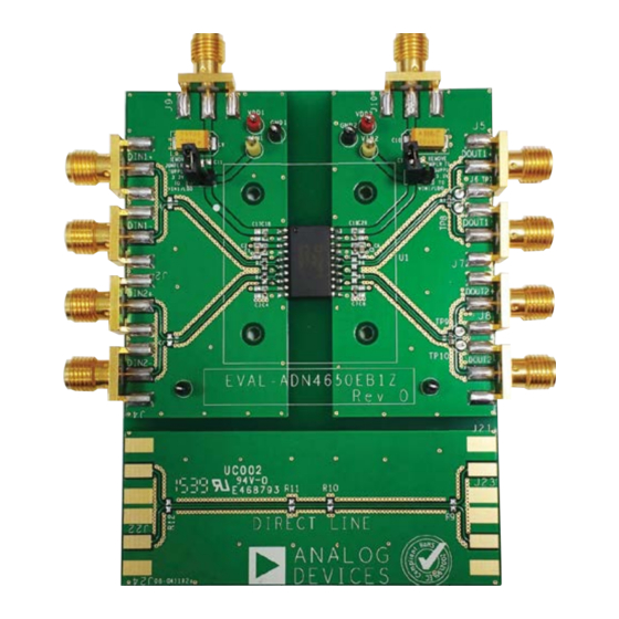
EVALUATION BOARD
Figure 1.
Rev. 0 | Page 1 of 9
allows quick and easy evaluation of
ADN4650
is capable of running at
with galvanic isolation between both sides of
ADN4650
is available in the
UG-933
ADN4650
employs
Advertisement
Table of Contents

Related Manuals for Analog Devices EVAL-ADN4650EB1Z


Summary of Contents for Analog Devices EVAL-ADN4650EB1Z
-
Page 1: Features
) and Side 2 (V Ground on Side 1 (GND ) and Side 2 (GND Analog Devices, Inc., iCoupler® technology to combine a 2-channel LVDS input signals: D isolator with an LVDS receiver and driver into a single, 20-lead IN1+ IN1−... -
Page 2: Table Of Contents
UG-933 EVAL-ADN4650EB1Z User Guide TABLE OF CONTENTS Features ....................1 Setting Up the Evaluation Board ..........3 Evaluation Kit Contents ..............1 Radiated Emissions Test Results (EN 55022) ........5 Documents Needed ................1 Evaluation Board Schematic and Artwork ........6 Equipment Needed ................1 Ordering Information ...............9... -
Page 3: Evaluation Board Configuration
GND with 0.1 µF capacitors (C5and C7). Figure 4 shows an example operation of the EVAL-ADN4650EB1Z. SMA connectors expose all LVDS inputs and outputs (see Table 2 and Table 3). Connect a signal generator using the J1 and J2 connectors and set up a 300 MHz square wave clock with an amplitude of 350 mV and an offset of 1.2 V. - Page 4 UG-933 EVAL-ADN4650EB1Z User Guide SIGNAL 2.5V OR 3.3V 2.5V OR 3.3V GENERATOR SUPPLY SUPPLY OSCILLOSCOPE GND1 GND2 TP10 GND1 GND2 EVAL-ADN4650EB1Z Figure 4. Basic LVDS Isolator Evaluation Board Operation Table 1. Jumper Configuration Jumper Position Description Open 3.3 V power supply connected to Connector J9 for V Closed 2.5 V power supply connected to Connector J9, V...
-
Page 5: Radiated Emissions Test Results (En 55022)
The test results are shown in Table 4; a classification report is Radiated emissions testing is performed at an independent external test facility with the EVAL-ADN4650EB1Z. Evaluating available on request (please contact Analog Devices or the EVAL-ADN4650EB1Z to the EN 55022 standard is undertaken component distributor for support). -
Page 6: Evaluation Board Schematic And Artwork
UG-933 EVAL-ADN4650EB1Z User Guide EVALUATION BOARD SCHEMATIC AND ARTWORK AGND3 VIN2 VIN1 VDD1 VDD2 TP40 DECOUPLING AGND1 AGND2 AGND1 VIN1 VIN2 AGND2 VDD1 AGND1 AGND2 AGND1 AGND2 20 PIN SOIC WB TP41 TP42 AGND1 AGND2 AGND2 AGND1 AGND1 AGND2 Figure 6. - Page 7 EVAL-ADN4650EB1Z User Guide UG-933 Figure 8. EVAL-ADN4650EB1Z Component Side Figure 9. EVAL-ADN4650EB1Z Inner Layer 2, Ground Rev. 0 | Page 7 of 9...
- Page 8 UG-933 EVAL-ADN4650EB1Z User Guide Figure 10. EVAL-ADN4650EB1Z Inner Layer 3, Power Figure 11. EVAL-ADN4650EB1Z Solder Side Rev. 0 | Page 8 of 9...
-
Page 9: Ordering Information
By using the evaluation board discussed herein (together with any tools, components documentation or support materials, the “Evaluation Board”), you are agreeing to be bound by the terms and conditions set forth below (“Agreement”) unless you have purchased the Evaluation Board, in which case the Analog Devices Standard Terms and Conditions of Sale shall govern. Do not use the Evaluation Board until you have read and agreed to the Agreement. - Page 10 Mouser Electronics Authorized Distributor Click to View Pricing, Inventory, Delivery & Lifecycle Information: Analog Devices Inc. EVAL-ADN4650EB1Z EVAL-ADN4650EBZ...
Need help?
Do you have a question about the EVAL-ADN4650EB1Z and is the answer not in the manual?
Questions and answers