Table of Contents
Advertisement
Quick Links
RD9Z1-638BJBEVM
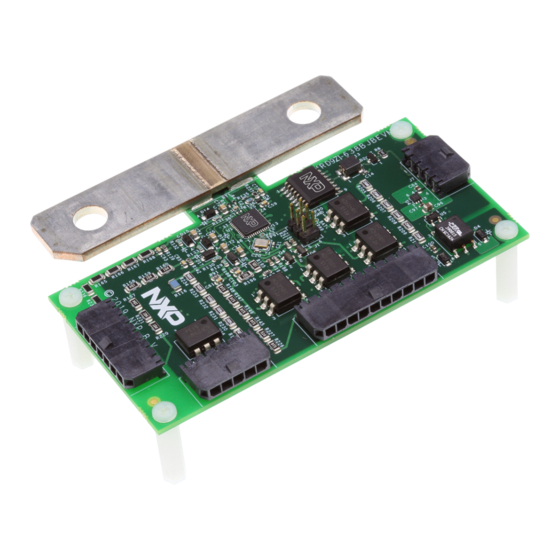
Figure 1. RD9Z1-638BJBEVM
Important Notice
NXP provides the enclosed product(s) under the following conditions:
This reference design is intended for use of ENGINEERING DEVELOPMENT OR EVALUATION PURPOSES ONLY. It is provided as a
sample IC pre-soldered to a printed circuit board to make it easier to access inputs, outputs, and supply terminals. This reference design
may be used with any development system or other source of I/O signals by simply connecting it to the host MCU or computer board via
off-the-shelf cables. Final device in an application will be heavily dependent on proper printed circuit board layout and heat sinking design
as well as attention to supply filtering, transient suppression, and I/O signal quality.
The goods provided may not be complete in terms of required design, marketing, and or manufacturing related protective considerations,
including product safety measures typically found in the end product incorporating the goods. Due to the open construction of the product,
it is the user's responsibility to take any and all appropriate precautions with regard to electrostatic discharge. In order to minimize risks
associated with the customers applications, adequate design and operating safeguards must be provided by the customer to minimize
inherent or procedural hazards. For any safety concerns, contact NXP sales and technical support services.
Should this reference design not meet the specifications indicated in the kit, it may be returned within 30 days from the date of delivery and
will be replaced by a new kit.
NXP reserves the right to make changes without further notice to any products herein. NXP makes no warranty, representation or
guarantee regarding the suitability of its products for any particular purpose, nor does NXP assume any liability arising out of the
application or use of any product or circuit, and specifically disclaims any and all liability, including without limitation consequential or
incidental damages. Typical parameters can and do vary in different applications and actual performance may vary over time. All operating
parameters, including Typical, must be validated for each customer application by customer's technical experts.
NXP does not convey any license under its patent rights nor the rights of others. NXP products are not designed, intended, or authorized
for use as components in systems intended for surgical implant into the body, or other applications intended to support or sustain life, or
for any other application in which the failure of the NXP product could create a situation where personal injury or death may occur.
Should the Buyer purchase or use NXP products for any such unintended or unauthorized application, the Buyer shall indemnify and hold
NXP and its officers, employees, subsidiaries, affiliates, and distributors harmless against all claims, costs, damages, and expenses, and
reasonable attorney fees arising out of, directly or indirectly, any claim of personal injury or death associated with such unintended or
unauthorized use, even if such claim alleges NXP was negligent regarding the design or manufacture of the part.
UM11396
RD9Z1-638BJBEVM Reference Design
Rev. 1 — 15 April 2020
User manual
Advertisement
Table of Contents

Subscribe to Our Youtube Channel
Related Manuals for NXP Semiconductors RD9Z1-638BJBEVM


Summary of Contents for NXP Semiconductors RD9Z1-638BJBEVM
-
Page 1: Fig. 1. Rd9Z1-638Bjbevm
UM11396 RD9Z1-638BJBEVM Reference Design Rev. 1 — 15 April 2020 User manual RD9Z1-638BJBEVM Figure 1. RD9Z1-638BJBEVM Important Notice NXP provides the enclosed product(s) under the following conditions: This reference design is intended for use of ENGINEERING DEVELOPMENT OR EVALUATION PURPOSES ONLY. It is provided as a sample IC pre-soldered to a printed circuit board to make it easier to access inputs, outputs, and supply terminals. -
Page 2: Introduction
• Design Resources – All of the information and resources required by users who have already purchased the RD9Z1-638BJBEVM reference design. This section includes: – RD9Z1-638BJBEVM - Getting Started – Click on this link for information on setting up the hardware, configuring the software and running an evaluation. -
Page 3: Additional Hardware
This evaluation board must be connected to a PC workstation running 32-bit and 64-bit versions of Windows 7 or above. 3.4 Software Using the RD9Z1-638BJBEVM board requires that the software listed below be installed on the PC workstation. The reference design projects are available on the RD9Z1-638BJBEVM tool summary page at http://www.nxp.com/RD9Z1-638BJBEVM. -
Page 4: Fig. 2. Rd9Z1-638Bjbevm Block Diagram
SYSTEM PUD/BDU HV Domain LV Domain OUTLINE aaa-037026 Figure 2. RD9Z1-638BJBEVM block diagram UM11396 All information provided in this document is subject to legal disclaimers. © NXP B.V. 2020. All rights reserved. User manual Rev. 1 — 15 April 2020 4 / 20... -
Page 5: Rd9Z1-638Bjbevm Board Components
UM11396 NXP Semiconductors RD9Z1-638BJBEVM Reference Design 4.3 Board components Figure 3. RD9Z1-638BJBEVM board components Table 1. RD9Z1-638BJBEVM board components No. Label Device Description Features MM9Z1_638 Intelligent • Wide range of battery current measurements; Battery On-chip temperature measurement Sensor • Four battery voltage measurements with internal resistor dividers;... - Page 6 UM11396 NXP Semiconductors RD9Z1-638BJBEVM Reference Design No. Label Device Description Features High-voltage 1x5 power Table 4 connector 1 plug connector High-voltage 1x10 Table 6 connector 3 power plug connector Panasonic MOSFET −U50 AQV258HAX relay TI SN6501 Push- AEC-Q qualified QDBVRQ1...
-
Page 7: Tab. 2. Bdm Connector (J1)
UM11396 NXP Semiconductors RD9Z1-638BJBEVM Reference Design 4.4 Connectors The RD9Z1-638BJBEVM board has five user-accessible connectors. Table 2 – Table 6 describe the pin functions for each connector. Table 2. BDM Connector (J1) Signal name Description J1_1 BKGD Connects to MM9Z1_638 BKGD pin to support background debug... -
Page 8: Test Points
MM9Z1_638 TP91 Test point for connection to MM9Z1_638 PA3 general purpose port 4.6 Configuring the hardware for setup using the RD9Z1-638BJBEVM board This section describes how to configure the hardware required to use the RD9Z1-638BJBEVM board in an evaluation environment. -
Page 9: Fig. 4. Hardware Configuration
4.6.2 Configuring the high-voltage domain Configuring the kit's high-voltage components consists of the following steps. 1. Open high-voltage connector 1 (J8) on the RD9Z1-638BJBEVM board and attach the 5-pin connector cable as follows: • Connect J8_1 to the HV ground. -
Page 10: Configuring The Low-Voltage Domain
If a previous version of CodeWarrior exists on the PC attached to the RD9Z1-638BJBEVM board, check to assure that the version is at least 10.2 or later. If CodeWarrior has not been installed, the following steps describe the installation process. -
Page 11: Importing The Reference Design Software
Graphical User Interface (GUI) than by a full- blown IDE such as CodeWarrior. Third-party USB-CAN tools and GUI development tools are available that allow RD9Z1-638BJBEVM reference design kit users to develop a GUI compatible with the RD9Z1-638BJBEVM board. -
Page 12: Fig. 5. Ldo
Hardware Design Guidelines The RD9Z1-638BJBEVM board is seperated into a low-voltage and a high-voltage domain. The board supports current measurement, high-voltage measurement, temperature measurement and insulation resistance measurement. 7.1 Power supply VCC_CAN +12 V_LV TPS70950QDRVRQ1... -
Page 13: Fig. 6. Power Supply For Mm9Z1_638
4. R177 or R178 can be placed as shown in Figure 7 to measure the HV-load current or the HV load current + the RD9Z1-638BJBEVM board current. UM11396 All information provided in this document is subject to legal disclaimers. © NXP B.V. 2020. All rights reserved. -
Page 14: Temperature Measurement
UM11396 NXP Semiconductors RD9Z1-638BJBEVM Reference Design 7.3 Temperature measurement VDDA R138 47 kΩ PTB4 R135 4 PTB4 2.2 kΩ R237 2200 pF 39 kΩ 10 kΩ R136 PTB5 4 PTB5 1 kΩ MM5Z5V1ST1G 2200 pF aaa-037130 Figure 8. Onboard TSENSE 1. RT1 is a temperature sensor used to monitor the temperature of the SHUNT resistor. -
Page 15: High-Voltage Measurement
UM11396 NXP Semiconductors RD9Z1-638BJBEVM Reference Design 7.4 High-voltage measurement Figure 9. High-voltage measurement 1. High voltage sensing point A, B, C, D, E, F, G and H inputs are around 1000 V. 2. The voltage tolerance of the divider resistor must be considered. Use a footprint of 1206 or larger. -
Page 16: Insulation Resistance Measurement
UM11396 NXP Semiconductors RD9Z1-638BJBEVM Reference Design 7.5 Insulation resistance measurement kΩ Y cap RISO+ chassis Y cap RISO- kΩ aaa-037131 Figure 10. Insulation resistance measurement 1. Close K1 to measure the voltage of R5(UR5) by AN+, to get a voltage V1. -
Page 17: Software Block
UM11396 NXP Semiconductors RD9Z1-638BJBEVM Reference Design 8.1 Software block Start Init Clk, interrupt, IO... Start continuous ADC Main loop Start Read current and voltage ADC finished? measurement result Read temperature 100 ms flag set? measurement result Send measurement Calculate insulation... -
Page 18: Legal Information
UM11396 NXP Semiconductors RD9Z1-638BJBEVM Reference Design 10 Legal information inclusion and/or use of NXP Semiconductors products in such equipment or applications and therefore such inclusion and/or use is at the customer's own 10.1 Definitions risk. Export control — This document as well as the item(s) described herein Draft —... -
Page 19: Table Of Contents
CAN communication protocol ......12 Figures Fig. 1. RD9Z1-638BJBEVM ..........1 Fig. 7. Current Sensing ..........13 Fig. 2. RD9Z1-638BJBEVM block diagram ....4 Fig. 8. Onboard TSENSE ........... 14 Fig. 3. RD9Z1-638BJBEVM board components ...5 Fig. 9. High-voltage measurement ......15 Fig. - Page 20 Kit contents ............2 Additional hardware ........... 3 Windows PC workstation ........3 Software .............3 Getting to Know the Hardware ......3 RD9Z1-638BJBEVM features ......3 Block diagram ............4 Board components ..........5 Connectors ............7 Test points ............8 Configuring the hardware for setup using the RD9Z1-638BJBEVM board ........8...
Need help?
Do you have a question about the RD9Z1-638BJBEVM and is the answer not in the manual?
Questions and answers