Table of Contents
Advertisement
Quick Links
UM11653
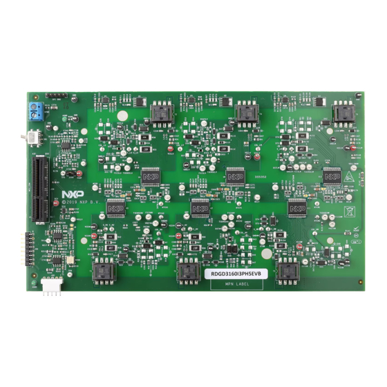
RDGD3160I3PH5EVB Reference Design
Rev. 1 — 12 August 2021
Document information
Information
Content
Keywords
RDGD3160I3PH5EVB, GD3160, MPC5777C-DEVB, MPC5744P, MPC5775B/
E-EVB, S32S Design Studio SDK, FreeMASTER, AMMCL, MCAT
Abstract
This document is the user guide for the RDGD3160I3PH5EVB reference
design and is intended for the engineers involved in the evaluation, design,
implementation, and validation of single-channel gate driver for IGBT,
GD3160.
User manual
Advertisement
Table of Contents

Related Manuals for NXP Semiconductors UM11653


Summary of Contents for NXP Semiconductors UM11653
- Page 1 UM11653 RDGD3160I3PH5EVB Reference Design Rev. 1 — 12 August 2021 User manual Document information Information Content Keywords RDGD3160I3PH5EVB, GD3160, MPC5777C-DEVB, MPC5744P, MPC5775B/ E-EVB, S32S Design Studio SDK, FreeMASTER, AMMCL, MCAT Abstract This document is the user guide for the RDGD3160I3PH5EVB reference...
- Page 2 UM11653 NXP Semiconductors RDGD3160I3PH5EVB Reference Design Revision History Revision history Date Description RDGD3160I3PH5EVB v.1 20210812 Initial version UM11653 All information provided in this document is subject to legal disclaimers. © NXP B.V. 2021. All rights reserved. User manual Rev. 1 — 12 August 2021...
- Page 3 UM11653 NXP Semiconductors RDGD3160I3PH5EVB Reference Design Important notice NXP provides the enclosed product(s) under the following conditions: This reference design is intended for use of ENGINEERING DEVELOPMENT OR EVALUATION PURPOSES ONLY. It is provided as a sample IC pre-soldered to a printed circuit board to make it easier to access inputs, outputs, and supply terminals.
-
Page 4: Introduction
NXP Semiconductors provides online resources for this reference design and its supported device(s) on http://www.nxp.com. The information page for RDGD3160I3PH5EVB reference design is at www.nxp.com/ RDGD3160I3PH5EVB. -
Page 5: Additional Hardware
UM11653 NXP Semiconductors RDGD3160I3PH5EVB Reference Design 3.2 Additional hardware In addition to the kit contents, the following hardware is necessary or beneficial when working with this kit. • Microcontroller for SPI communication • IGBT module Infineon HP Drive part FS820R08A6P2B •... -
Page 6: Voltage Domains, Gd3160 Pinout, Logic Header, And Igbt Pinout
UM11653 NXP Semiconductors RDGD3160I3PH5EVB Reference Design 4.1.2 Voltage domains, GD3160 pinout, logic header, and IGBT pinout Low-voltage domain is an externally supplied 12 V DC (VSUP) primary supply for non- isolated circuits, typically supplied by vehicle battery. The low-voltage domain includes the interface between the MCU and GD3160 control registers and logic control. -
Page 7: Gd3160 Pinout And Mcu Interface Pinout
UM11653 NXP Semiconductors RDGD3160I3PH5EVB Reference Design • Interrupt pin for fast response to faults • Compatible with negative gate supply • Compatible with 200 V to 1700 V IGBTs, power range > 125 kW • AEC-Q100 grade 1 qualified 4.2.2 GD3160 pinout and MCU interface pinout See GD3160 advanced IGBT/SiC gate driver data sheet for specific information about pinout, pin descriptions, specifications, and operating modes. - Page 8 UM11653 NXP Semiconductors RDGD3160I3PH5EVB Reference Design Table 1. PCIe connector pin definitions Name Function VDDA Voltage reference resolver circuit GNDA1 Analog ground PH_U_I Current feedback phase U PH_V_I Current feedback phase V PH_W_I Current feedback phase W n.c. not connected n.c.
-
Page 9: Test Points
UM11653 NXP Semiconductors RDGD3160I3PH5EVB Reference Design Table 1. PCIe connector pin definitions ...continued Name Function COS_N_OUT_RSLV Cosine resolver signal n.c. not connected GNDA3 Analog ground MCU_VCC MCU VCC regulator voltage GND1 Ground AOUTHU GD3160 analog output signal high-side U phase AOUTLU... - Page 10 UM11653 NXP Semiconductors RDGD3160I3PH5EVB Reference Design Figure 3. RDGD3160I3PH5EVB test points Test point name Function Micro DC voltage DSTHU DESAT high-side U phase V desaturation connected to DESAT pin circuitry DSTHV DESAT high-side V phase V desaturation connected to DESAT pin circuitry...
-
Page 11: Indicators
UM11653 NXP Semiconductors RDGD3160I3PH5EVB Reference Design Test point name Function TSENSEHW TSENSE high-side W phase connected to NTC temperature sense TSENSELU TSENSE low-side U phase TSENSELV TSENSE low-side V phase TSENSELW TSENSE low-side W phase 4.2.4 Indicators The RDGD3160I3PH5EVB evaluation board contains LEDs as visual indicators on the board. -
Page 12: Power Supply And Jumper Configuration
UM11653 NXP Semiconductors RDGD3160I3PH5EVB Reference Design Table 3. RDGD3160I3PH5EVB connector descriptions Name Description Phase current feedback connector Current feedback connections from U, V, and W phases Resolver signals connector Resolver excitation signals (see schematic for more information) 4.2.6 Power supply and jumper configuration Figure 6. Power supply and jumper locations... -
Page 13: Gate Drive Resistors
UM11653 NXP Semiconductors RDGD3160I3PH5EVB Reference Design Name Function VCCHV High-side phase V VCC voltage test point Isolated positive voltage supply (15 V to 18 V) VCCHW High-side phase W VCC voltage test point Isolated positive voltage supply (15 V to 18 V) -
Page 14: Igbt Pin Connections
UM11653 NXP Semiconductors RDGD3160I3PH5EVB Reference Design 4.2.8 IGBT pin connections Figure 8. IGBT connection pins Connection name Pin description COL_HU Collector high-side U phase COL_HV Collector high-side V phase COL_HW Collector high-side W phase COL_LU Collector low-side U phase COL_LV Collector low-side V phase... -
Page 15: Configuring The Hardware For Startup
UM11653 NXP Semiconductors RDGD3160I3PH5EVB Reference Design Configuring the hardware for startup Figure 9 presents a typical hardware configuration. Figure 9. Typical configuration To configure the hardware as illustrated in Figure 9, complete the following procedure: 1. Assemble IGBT module with water cooling jacket if desired and properly attach to DC Link capacitor positive and negative high-voltage supply connections across U, V, and W phases. -
Page 16: Installing And Configuring Software And Tools
UM11653 NXP Semiconductors RDGD3160I3PH5EVB Reference Design 5. Connect DC power: a. Connect a low voltage DC power supply to the RDGD3160I3H5EVB at the VSUP connection terminal (12 V DC with a minimum 1.0 A supply). Ensure that J100 jumper is in place. -
Page 17: References
UM11653 NXP Semiconductors RDGD3160I3PH5EVB Reference Design • S32S Design Studio IDE for power architecture: The S32S design studio for power architecture IDE installed on a Windows PC workstation enables editing, compiling and debugging of source code designs. SDK supports several devices including MPC5777C. For more information, refer to S32DS- PA SDK for power architectures at http://www.nxp.com/S32SDK-PA. -
Page 18: Legal Information
Customers agree to fully indemnify NXP Semiconductors 8.2 Disclaimers for any damages resulting from or in connection with such high voltages. - Page 19 UM11653 NXP Semiconductors RDGD3160I3PH5EVB Reference Design NXP — wordmark and logo are trademarks of NXP B.V. UM11653 All information provided in this document is subject to legal disclaimers. © NXP B.V. 2021. All rights reserved. User manual Rev. 1 — 12 August 2021...
- Page 20 UM11653 NXP Semiconductors RDGD3160I3PH5EVB Reference Design Tables Tab. 1. PCIe connector pin definitions ......8 Tab. 3. RDGD3160I3PH5EVB connector Tab. 2. RDGD3160I3PH5EVB indicator descriptions ............. 12 descriptions ............. 11 Figures Fig. 1. RDGD3160I3PH5EVB three-phase inverter Fig. 6. Power supply and jumper locations ....12 board voltage domains and interfaces ....
-
Page 21: Table Of Contents
'Legal information'. © NXP B.V. 2021. All rights reserved. For more information, please visit: http://www.nxp.com For sales office addresses, please send an email to: salesaddresses@nxp.com Date of release: 12 August 2021 Document identifier: UM11653...
Need help?
Do you have a question about the UM11653 and is the answer not in the manual?
Questions and answers