Table of Contents
Advertisement
Quick Links
FEATURES
Complete supervisory and sequencing solution for up to
10 supplies
10 supply fault detectors enable supervision of supplies to
<0.5% accuracy at all voltages at 25°C
<1.0% accuracy across all voltages and temperatures
5 selectable input attenuators allow supervision of supplies to
14.4 V on VH
6 V on VP1 to VP4 (VPx)
5 dual-function inputs, VX1 to VX5 (VXx)
High impedance input to supply fault detector with
thresholds between 0.573 V and 1.375 V
General-purpose logic input
10 programmable driver outputs, PDO1 to PDO10 (PDOx)
Open-collector with external pull-up
Push/pull output, driven to VDDCAP or VPx
Open collector with weak pull-up to VDDCAP or VPx
Internally charge-pumped high drive for use with external
N-FET (PDO1 to PDO6 only)
Sequencing engine (SE) implements state machine control
of PDOx outputs
State changes conditional on input events
Enables complex control of boards
Power-up and power-down sequence control
Fault event handling
Interrupt generation on warnings
Watchdog function can be integrated in SE
Program software control of sequencing through SMBus
Complete voltage margining solution for 6 voltage rails
12-bit ADC for readback of all supervised voltages
1 internal and 2 external temperature sensors
Reference input (REFIN) has 2 input options
Driven directly from 2.048 V (±0.25%) REFOUT pin
More accurate external reference for improved
ADC performance
Device powered by the highest of VPx, VH for improved
redundancy
User EEPROM: 256 bytes
Industry-standard, 2-wire bus interface (SMBus)
Guaranteed PDO low with VH, VPx = 1.2 V
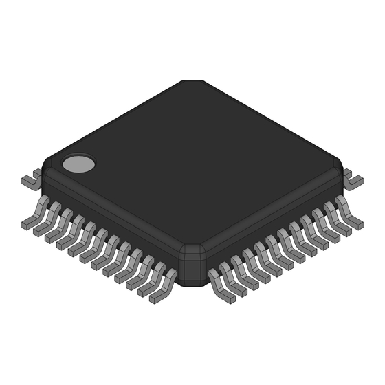
Available in 40-lead, 6 mm × 6 mm LFCSP and
48-lead, 7 mm × 7 mm TQFP packages
For more information about the ADM1063 register map,
refer to the AN-698 Application Note at www.analog.com.
Rev. C
Information furnished by Analog Devices is believed to be accurate and reliable. However, no
responsibility is assumed by Analog Devices for its use, nor for any infringements of patents or other
rights of third parties that may result from its use. Specifications subject to change without notice. No
license is granted by implication or otherwise under any patent or patent rights of Analog Devices.
Trademarks and registered trademarks are the property of their respective owners.
Multisupply Supervisor/Sequencer with
ADC and Temperature Monitoring
D1P
VX1
VX2
VX3
VX4
VX5
VP1
VP2
VP3
VP4
VH
AGND
APPLICATIONS
Central office systems
Servers/routers
Multivoltage system line cards
DSP/FPGA supply sequencing
In-circuit testing of margined supplies
GENERAL DESCRIPTION
The ADM1063 is a configurable supervisory/sequencing device
that offers a single-chip solution for supply monitoring and
sequencing in multiple supply systems. In addition to these
functions, the ADM1063 integrates a 12-bit ADC that can be
used to accurately read back up to 12 separate voltages.
The device also provides up to 10 programmable inputs for
monitoring undervoltage faults, overvoltage faults, or out-of-
window faults on up to 10 supplies. In addition, 10 programmable
outputs can be used as logic enables. Six of these programmable
outputs can provide up to a 12 V output for driving the gate of
an N-FET that can be placed in the path of a supply.
One Technology Way, P.O. Box 9106, Norwood, MA 02062-9106, U.S.A.
Tel: 781.329.4700
Fax: 781.461.3113
FUNCTIONAL BLOCK DIAGRAM
D1N D2P
D2N
REFIN
REFOUT
REFGND
VREF
TEMP
INTERNAL
SENSOR
DIODE
12-BIT
SAR ADC
CLOSED-LOOP
MARGINING SYSTEM
DUAL-
FUNCTION
INPUTS
(LOGIC INPUTS
OR
SFDs)
SEQUENCING
ENGINE
PROGRAMMABLE
RESET
GENERATORS
(SFDs)
ADM1063
Figure 1.
©2005–2011 Analog Devices, Inc. All rights reserved.
ADM1063
SDA SCL A1
A0
SMBus
INTERFACE
EEPROM
PDO1
CONFIGURABLE
OUTPUT
PDO2
DRIVERS
PDO3
PDO4
(HV CAPABLE OF
PDO5
DRIVING GATES
OF N-FET)
PDO6
PDO7
CONFIGURABLE
OUTPUT
PDO8
DRIVERS
(LV CAPABLE
PDO9
OF DRIVING
LOGIC SIGNALS)
PDO10
PDOGND
VDD
VDDCAP
ARBITRATOR
VCCP
GND
www.analog.com
Advertisement
Table of Contents

Subscribe to Our Youtube Channel
Related Manuals for Analog Devices ADM1063


Summary of Contents for Analog Devices ADM1063
-
Page 1: Features
Information furnished by Analog Devices is believed to be accurate and reliable. However, no responsibility is assumed by Analog Devices for its use, nor for any infringements of patents or other One Technology Way, P.O. Box 9106, Norwood, MA 02062-9106, U.S.A. -
Page 2: Table Of Contents
Deleted Figure 17 to Figure 19............12 Changes to Table 1................4 Changes to Programming the Supply Fault Detectors Section... 14 Changes to Powering the ADM1063 Section ......13 Changes to Table 6................14 Changes to Table 5................14 Changes to Outputs Section............16 Changes to Default Output Configuration Section .... -
Page 3: Detailed Block Diagram
ADM1063 Temperature measurement is possible with the ADM1063. The This design enables very flexible sequencing of the outputs device contains one internal temperature sensor and two pairs based on the condition of the inputs. of differential inputs for remote thermal diodes. These are The device is controlled via configuration data that can be measured by the 12-bit ADC. -
Page 4: Specifications
ADM1063 SPECIFICATIONS VH = 3.0 V to 14.4 V , VPx = 3.0 V to 6.0 V = −40°C to +85°C, unless otherwise noted. Table 1. Parameter Unit Test Conditions/Comments POWER SUPPLY ARBITRATION VH, VPx Minimum supply required on one of VH, VPx Maximum VDDCAP = 5.1 V, typical... - Page 5 ADM1063 Parameter Unit Test Conditions/Comments Conversion Time 0.44 One conversion on one channel All 12 channels selected, 16× averaging enabled Offset Error ±2 = 2.048 V REFIN Input Noise 0.25 LSB rms Direct input (no attenuator) TEMPERATURE SENSOR Local Sensor Accuracy ±3...
- Page 6 ADM1063 Parameter Unit Test Conditions/Comments SERIAL BUS TIMING Clock Frequency, f SCLK Bus Free Time, t μs Start Setup Time, t μs SU;STA Stop Setup Time, t μs SU;STO Start Hold Time, t μs HD;STA SCL Low Time, t μs SCL High Time, t μs...
-
Page 7: Pin Configurations And Function Descriptions
ADM1063 PIN CONFIGURATIONS AND FUNCTION DESCRIPTIONS 48 47 46 45 44 43 42 41 40 39 38 37 PDO1 PIN 1 PIN 1 PDO1 INDICATOR PDO2 INDICATOR PDO2 PDO3 PDO3 PDO4 ADM1063 PDO4 PDO5 ADM1063 TOP VIEW PDO5 PDO6 (Not to Scale) - Page 8 ADM1063 Pin No. Mnemonic Description LFCSP TQFP External Temperature Sensor 1 Cathode Connection. External Temperature Sensor 1 Anode Connection. VDDCAP Device Supply Voltage. Linearly regulated from the highest of the VPx, VH pins to a typical of 4.75 V. Note that the capacitor must be connected between this pin and GND. A 10 μF capacitor is recommended for this purpose.
-
Page 9: Absolute Maximum Ratings
ADM1063 ABSOLUTE MAXIMUM RATINGS Table 3. Stresses above those listed under Absolute Maximum Ratings Parameter Rating may cause permanent damage to the device. This is a stress Voltage on VH Pin 16 V rating only; functional operation of the device at these or any... -
Page 10: Typical Performance Characteristics
ADM1063 TYPICAL PERFORMANCE CHARACTERISTICS Figure 5. V vs. V Figure 8. I vs. V (VP1 Not as Supply) VDDCAP Figure 6. V vs. V Figure 9. I vs. V (VH as Supply) VDDCAP Figure 10. I vs. V (VH Not as Supply) Figure 7. - Page 11 ADM1063 –0.2 –0.4 –0.6 –0.8 –1.0 10.0 12.5 15.0 1000 2000 3000 4000 (μA) CODE LOAD Figure 11. Charge-Pumped V (FET Drive Mode) vs. I Figure 14. DNL for ADC PDO1 LOAD VP1 = 5V VP1 = 3V –0.2 –0.4 –0.6...
-
Page 12: Deleted Figure 17 To Figure 19
ADM1063 2.058 2.053 VP1 = 3.0V 2.048 VP1 = 4.75V 2.043 2.038 –40 –20 TEMPERATURE (°C) Figure 17. REFOUT vs. Temperature Rev. C | Page 12 of 32... -
Page 13: Powering The Adm1063
There is minimal switching loss with this architecture (~0.2 V), resulting in the ability to power the 4.75V ADM1063 from a supply as low as 3.0 V. Note that the supply on the VXx pins cannot be used to power the device. 4.75V An external capacitor to GND is required to decouple the on-chip supply from noise. -
Page 14: Inputs
(as discussed in the AN-698 Application Note at www.analog.com) PROGRAMMING THE SUPPLY FAULT DETECTORS is given by The ADM1063 can have up to 10 SFDs on its 10 input channels. N = 255 × (5 − 2.5)/3.5 These highly programmable reset generators enable the supervision Therefore, N = 182 (1011 0110 or 0xB6). -
Page 15: Input Glitch Filtering
VXx input pins on the ADM1063 have dual functionality. process is shown in Figure 20. The second function is as a digital logic input to the device. Therefore, the ADM1063 can be configured for up to five digital INPUT PULSE SHORTER INPUT PULSE LONGER... -
Page 16: Outputs
SFDs are in tolerance, or a RESET output if one of the SFDs As the input supply to the ADM1063 ramps up on VPx or VH, goes out of specification (this can be used as a status signal for a all PDOx pins behave as follows: DSP, FPGA, or other microcontroller). -
Page 17: Sequencing Engine
Figure 23. State Cell and so on. A watchdog function that verifies the continued The ADM1063 offers up to 63 state definitions. The signals operation of a processor clock can be integrated into the SE monitored to indicate the status of the input pins are the program. -
Page 18: Sequencing Engine Application Example
ADM1063 If a timer delay is specified, the input to the sequence detector SEQUENCING ENGINE APPLICATION EXAMPLE must remain in the defined state for the duration of the timer The application in this section demonstrates the operation of delay. If the input changes state during the delay, the timer is reset. -
Page 19: Changes To Sequence Detector Section
FAULT AND STATUS REPORTING FAULT SUPPLY FAULT DETECTION The ADM1063 has a fault latch for recording faults. Two registers, FSTAT1 and FSTAT2, are set aside for this purpose. A single bit MASK SENSE is assigned to each input of the device, and a fault on that input sets the relevant bit. -
Page 20: Voltage Readback
Figure 27. ADC Reading on VXx Pins In addition to the readback capability, another level of supervi- sion is provided by the on-chip, 12-bit ADC. The ADM1063 has limit registers with which the user can program a maximum or ATTENUATION NETWORK... -
Page 21: Changes To Temperature Measurement System Section
DxN input and the base is connected to the DxP input. As with the other analog inputs to the ADC, a limit register is Figure 29 and Figure 30 show how to connect the ADM1063 provided for each of the temperature input channels. Therefore, to an NPN or PNP transistor for temperature measurement. -
Page 22: Changes To Table 10
ADM1063 To measure ΔV , the sensor is switched between operating Table 10. Temperature Data Format currents of I and N × I. The resulting waveform is passed through Temperature Digital Output (Hex) Digital Output (Binary) a 65 kHz low-pass filter to remove noise and through a chopper- −128°C... -
Page 23: Applications Diagram
ADM1063 APPLICATIONS DIAGRAM 12V IN 12V OUT 5V IN 5V OUT 3V IN 3V OUT DC-TO-DC1 3.3V OUT ADM1063 5V OUT PDO1 3V OUT PDO2 3.3V OUT 2.5V OUT DC-TO-DC2 PDO3 1.8V OUT 1.2V OUT PDO4 2.5V OUT 0.9V OUT... -
Page 24: Changes To Configuration Download At Power-Up Section
ADM1063 COMMUNICATING WITH THE ADM1063 The ADM1063 provides several options that allow the user to CONFIGURATION DOWNLOAD AT POWER-UP update the configuration over the SMBus interface. The following The configuration of the ADM1063 (undervoltage/overvoltage three options are controlled in the UPDCFG register. -
Page 25: Changes To Table 11
Page 0 to Page 6, starting at Address 0xF800, hold the configuration To alter a state, the required changes must be made directly to data for the applications on the ADM1063 (such as the SFDs and the EEPROM. RAM for each state does not exist. The relevant PDOs). - Page 26 Address Value Function MANID 0xF4 0x41 Manufacturer ID for Analog Devices Data is sent over the serial bus in sequences of nine clock pulses: REVID 0xF5 0x02 Silicon revision eight bits of data followed by an acknowledge bit from the slave...
-
Page 27: Smbus Protocols For Ram And Eeprom
Page erasure is enabled by setting Bit 2 in the UPDCFG register (Address 0x90) to 1. If this bit is not set, page erasure cannot In the ADM1063, the send byte protocol is used for two purposes: occur, even if the command byte (0xFE) is programmed across •... -
Page 28: Changes To Identifying The Adm1063 On The Smbus Section
ADM1063 The master sends a command code telling the slave device to erase EEPROM EEPROM the page. The ADM1063 command code for a page erasure is 0xFE SLAVE ADDRESS ADDRESS ADDRESS HIGH BYTE LOW BYTE (1111 1110). Note that for a page erasure to take place, the page... -
Page 29: Changes To Figure 44 And Error Correction Section
RAM/ EEPROM. This option enables the user to verify transaction ends. that the data received by or sent from the ADM1063 is correct. The PEC byte is an optional byte sent after the last data byte has In the ADM1063, the receive byte protocol is used to read a been written to or read from the ADM1063. -
Page 30: Added Exposed Pad Notation To Outline Dimensions
ADM1063 OUTLINE DIMENSIONS 6.00 0.60 MAX BSC SQ 0.60 MAX PIN 1 INDICATOR PIN 1 0.50 INDICATOR 4.25 5.75 EXPOSED VIEW 4.10 SQ BSC SQ 3.95 (BOT TOM VIEW) 0.50 0.40 0.30 0.25 MIN 4.50 12° MAX 0.80 MAX 0.65 TYP FOR PROPER CONNECTION OF 0.05 MAX... -
Page 31: Changes To Ordering Guide
ADM1063 ORDERING GUIDE Model Temperature Range Package Description Package Option ADM1063ACPZ −40°C to +85°C 40-Lead LFCSP_VQ CP-40-1 ADM1063ACPZ-REEL7 −40°C to +85°C 40-Lead LFCSP_VQ CP-40-1 ADM1063ASUZ −40°C to +85°C 48-Lead TQFP SU-48 ADM1063ASUZ-REEL7 −40°C to +85°C 48-Lead TQFP SU-48 EVAL-ADM1063TQEBZ Evaluation Kit (TQFP Version) Z = RoHS Compliant Part. - Page 32 ADM1063 NOTES ©2005–2011 Analog Devices, Inc. All rights reserved. Trademarks and registered trademarks are the property of their respective owners. D04632-0-7/11(C) Rev. C | Page 32 of 32...
Need help?
Do you have a question about the ADM1063 and is the answer not in the manual?
Questions and answers