Table of Contents
Advertisement
Quick Links
FEATURES
Complete supervisory and sequencing solution for up to
10 supplies
10 supply fault detectors enable supervision of supplies to
better than 1% accuracy
5 selectable input attenuators allow supervision of
supplies up to
14.4 V on VH
6 V on VP1 to VP4
5 dual-function inputs, VX1 to VX5
High impedance input to supply fault detector with
thresholds between 0.573 V and 1.375 V
General-purpose logic input
10 programmable output drivers, PDO1 to PDO10
Open collector with external pull-up
Push/pull output, driven to VDDCAP or VPn
Open collector with weak pull-up to VDDCAP or VPn
Internally charge-pumped high drive for use with external
N-FET (PDO1 to PDO6 only)
Sequencing engine (SE) implements state machine control of
PDO outputs
State changes conditional on input events
Enables complex control of boards
Power-up and power-down sequence control
Fault event handling
Interrupt generation on warnings
Watchdog function can be integrated in SE
Program software control of sequencing through SMBus
Complete voltage margining solution for 6 voltage rails
6 voltage output, 8-bit DACs (0.300 V to 1.551 V) allow voltage
adjustment via dc-to-dc converter trim/feedback node
12-bit ADC for readback of all supervised voltages
1 internal and 2 external temperature sensors
Reference input, REFIN, has 2 input options
Driven directly from 2.048 V (±0.25%) REFOUT pin
More accurate external reference for improved
ADC performance
Device powered by the highest of VP1 to VP4, VH for
improved redundancy
User EEPROM: 256 bytes
Industry-standard, 2-wire bus interface (SMBus)
Guaranteed PDO low with VH, VPn = 1.2 V
40-lead, 6 mm × 6 mm LFCSP and
48-lead, 7 mm × 7 mm TQFP packages
Rev. 0
Information furnished by Analog Devices is believed to be accurate and reliable.
However, no responsibility is assumed by Analog Devices for its use, nor for any
infringements of patents or other rights of third parties that may result from its use.
Specifications subject to change without notice. No license is granted by implication
or otherwise under any patent or patent rights of Analog Devices. Trademarks and
registered trademarks are the property of their respective owners.
Multisupply Supervisor/Sequencer
with ADC and Temperature Monitoring
FUNCTIONAL BLOCK DIAGRAM
D1P
D1N D2P
TEMP
SENSOR
CLOSED-LOOP
MARGINING SYSTEM
VX1
VX2
VX3
(LOGIC INPUTS
VX4
VX5
VP1
PROGRAMMABLE
VP2
VP3
GENERATORS
VP4
VH
AGND
APPLICATIONS
Central office systems
Servers/routers
Multivoltage system line cards
DSP/FPGA supply sequencing
In-circuit testing of margined supplies
GENERAL DESCRIPTION
The ADM1063 is a configurable supervisory/sequencing device
that offers a single-chip solution for supply monitoring and
sequencing in multiple supply systems. In addition to these
functions, the ADM1063 integrates a 12-bit ADC and six 8-bit
voltage output DACs. These circuits can be used to implement a
closed-loop margining system, which enables supply adjustment
by altering either the feedback node or reference of a dc-to-dc
converter using the DAC outputs.
One Technology Way, P.O. Box 9106, Norwood, MA 02062-9106, U.S.A.
Tel: 781.329.4700
Fax: 781.461.3113
D2N
REFIN
REFOUT
REFGND
SDA SCL A1
VREF
INTERNAL
DIODE
ADM1063
12-BIT
SAR ADC
CONFIGURABLE
DUAL-
FUNCTION
INPUTS
OR
SFDs)
N-CHANNEL FET)
SEQUENCING
ENGINE
CONFIGURABLE
RESET
(SFDs)
LOGIC SIGNALS)
VCCP
Figure 1.
© 2005 Analog Devices, Inc. All rights reserved.
ADM1063
A0
SMBus
INTERFACE
EEPROM
PDO1
OUTPUT
PDO2
DRIVERS
PDO3
(HV CAPABLE
PDO4
OF DRIVING
PDO5
GATES OF
PDO6
PDO7
OUTPUT
DRIVERS
PDO8
(LV CAPABLE
PDO9
OF DRIVING
PDO10
PDOGND
VDD
VDDCAP
ARBITRATOR
GND
(continued on Page 3)
www.analog.com
Advertisement
Table of Contents

Related Manuals for Analog Devices ADM1063


Summary of Contents for Analog Devices ADM1063
- Page 1 Information furnished by Analog Devices is believed to be accurate and reliable. However, no responsibility is assumed by Analog Devices for its use, nor for any infringements of patents or other rights of third parties that may result from its use.
-
Page 2: Table Of Contents
ESD Caution.................. 8 Open-Loop Margining .............. 21 Typical Performance Characteristics ..........9 Closed-Loop Supply Margining ..........21 Powering the ADM1063 ..............12 Writing to the DACs ..............22 Inputs....................13 Choosing the Size of the Attenuation Resistor....... 22 Supply Supervision..............13 DAC Limiting and Other Safety Features ....... -
Page 3: General Description
GENERAL DESCRIPTION (continued from Page 1) Supply margining can be performed with a minimum of Temperature measurement is possible with the ADM1063. The external components. The margining loop can be used for device contains one internal temperature sensor and two pairs in-circuit testing of a board during production (for example, to of differential inputs for remote thermal diodes. -
Page 4: Specifications
ADM1063 SPECIFICATIONS VH = 3.0 V to 14.4 V , VPn = 3.0 V to 6.0 V = −40°C to +85°C, unless otherwise noted. Table 1. Parameter Unit Test Conditions/Comments POWER SUPPLY ARBITRATION VH, VPn Minimum supply required on one of VH, VPn. - Page 5 ADM1063 Parameter Unit Test Conditions/Comments Conversion Time 0.44 One conversion on one channel All 12 channels selected, 16x averaging enabled Offset Error ±2 = 2.048 V REFIN Input Noise 0.25 Direct input (no attenuator) TEMPERATURE SENSOR Local Sensor Accuracy ±3 °C...
- Page 6 ADM1063 Parameter Unit Test Conditions/Comments Standard (Digital Output) Mode (PDO1 to PDO10) (pull-up to VDDCAP or VPn) = 2.7 V, I = 0.5 mA to VPn = 6.0 V, I = 0 mA − 0.3 ≤ 2.7 V, I = 0.5 mA 0.50...
-
Page 7: Pin Configurations And Function Descriptions
ADM1063 PIN CONFIGURATIONS AND FUNCTION DESCRIPTIONS 48 47 46 45 44 43 42 41 40 39 38 37 PIN 1 PDO1 INDICATOR PDO1 PDO2 PIN 1 PDO2 INDICATOR PDO3 PDO3 PDO4 PDO4 ADM1063 PDO5 ADM1063 PDO5 TOP VIEW PDO6 TOP VIEW... -
Page 8: Absolute Maximum Ratings
ADM1063 ABSOLUTE MAXIMUM RATINGS Table 3. Stresses above those listed under Absolute Maximum Ratings Parameter Rating may cause permanent damage to the device. This is a stress Voltage on VH Pin 16 V rating only; functional operation of the device at these or any... -
Page 9: Typical Performance Characteristics
ADM1063 TYPICAL PERFORMANCE CHARACTERISTICS Figure 5. V vs. V Figure 8. I vs. V (VP1 Not as Supply) VDDCAP Figure 9. I vs. V (VH as Supply) Figure 6. V vs. V VDDCAP Figure 7. I vs. V (VP1 as Supply) Figure 10. - Page 10 ADM1063 –0.2 –0.4 –0.6 –0.8 –1.0 10.0 12.5 15.0 1000 2000 3000 4000 ( µ A) CODE LOAD Figure 11. Charge-Pumped V (FET Drive Mode) vs. I Figure 14. DNL for ADC PDO1 LOAD VP1 = 5V VP1 = 3V –0.2...
- Page 11 ADM1063 1.005 1.004 1.003 1.002 1.001 VP1 = 3.0V 1.000 VP1 = 4.75V 0.999 20kΩ BUFFER PROBE OUTPUT 47pF POINT 0.998 0.997 0.996 0.995 –40 –20 200mV M1.00µs 756mV TEMPERATURE (°C) Figure 17. Transient Response of DAC Code Change into Typical Load Figure 19.
-
Page 12: Powering The Adm1063
4.75V supply. There is minimal switching loss with this architecture (~0.2 V), resulting in the ability to power the ADM1063 from a INTERNAL DEVICE supply as low as 3.0 V. Note that the supply on the VXn pins SUPPLY 4.75V... -
Page 13: Inputs
PROGRAMMING THE SUPPLY FAULT DETECTORS Reversing the equation, the code for a desired threshold is given by The ADM1063 can have up to 10 SFDs on its 10 input channels. These highly programmable reset generators enable N = 255 × (V −... -
Page 14: Input Comparator Hysteresis
This allows the user to remove any spurious transitions, such as of the VXn pin and supervised. This enables the ADM1063 to supply bounce at turn-on. The glitch filter function is additional monitor other supplies such as +24 V, +48 V, and −5 V. -
Page 15: Vxn Pins As Digital Inputs
Therefore, the ADM1063 can be configured for up to five digital inputs. These When configured as digital inputs, each of the VXn pins has a inputs are TTL-/CMOS-compatible. -
Page 16: Outputs
(SE). The SE determines what action is taken with the • Output from the SE. PDOs based on the condition of the inputs of the ADM1063. • Directly from the SMBus. A PDO can be configured so that Therefore, the PDOs can be set up to assert when the SFDs are in tolerance, the correct input signals are received on the VXn the SMBus has direct control over it. -
Page 17: Sequencing Engine
Figure 26. State Cell operation of a processor clock can be integrated into the SE The ADM1063 offers up to 63 state definitions. The signals program. The SE can also be controlled via the SMBus, giving monitored to indicate the status of the input pins are the software or firmware control of the board sequencing. -
Page 18: Sequencing Engine Application Example
ADM1063 SEQUENCE SEQUENCING ENGINE APPLICATION EXAMPLE STATES The application in this section demonstrates the operation of the SE. Figure 27 shows how the simple building block of a IDLE1 single SE state can be used to build a power-up sequence for a 3-supply system. -
Page 19: Sequence Detector
FAULT REPORTING state configuration to download from EEPROM into the SE. The ADM1063 has a fault latch for recording faults. Two registers Figure 29 is a block diagram of the monitoring fault detector. are set aside for this purpose. A single bit is assigned to each input of the device, and a fault on that input sets the relevant bit. -
Page 20: Voltage Readback
In addition to the readback capability, a further level of supervi- Figure 30. ADC Reading on VXn Pins sion is provided by the on-chip, 12-bit ADC. The ADM1063 has limit registers on which the user can program a maximum or minimum allowable threshold. -
Page 21: Supply Margining
Step 1 to Step 3 ensure that when the DACn output buffer is turned on, it has little effect on the dc-to-dc output. The DAC The ADM1063 can be commanded to margin a supply up or output buffer is designed to power up without glitching by first down over the SMBus by updating the values on the relevant powering up the buffer to follow the pin voltage. -
Page 22: Writing To The Dacs
ADM1063 means that the current flowing through R1 is the same as the WRITING TO THE DACs current flowing through R3. Therefore, a direct relationship Four DAC ranges are offered. They can be placed with midcode exists between the extra voltage drop across R1 during margining (Code 0x7F) at 0.6 V, 0.8 V, 1.0 V, and 1.25 V. -
Page 23: Temperature Measurement System
DxN input and the base is connected to the DxP input. of the device, local temperature measurements outside this Figure 35 and Figure 36 show how to connect the ADM1063 range are not possible. Temperature measurements from to an NPN or PNP transistor for temperature measurement. To −128°C to +127°C are possible using a remote sensor. - Page 24 ADM1063 × BIAS OUT+ THERM DA REMOTE TO ADC THERM DC SENSING TRANSISTOR BIAS OUT– DIODE LOW-PASS FILTER = 65kHz Figure 34. Signal Conditioning for Remote Diode Temperature Sensors ADM1063 ADM1063 2N3904 2N3906 Figure 35. Measuring Temperature Using an NPN Transistor Figure 36.
-
Page 25: Applications Diagram
ADM1063 APPLICATIONS DIAGRAM 12V IN 12V OUT 5V IN 5V OUT 3V IN 3V OUT DC-DC1 3.3V OUT ADM1063 5V OUT PDO1 3V OUT PDO2 3.3V OUT 2.5V OUT DC-DC2 PDO3 1.8V OUT 1.2V OUT PDO4 2.5V OUT 0.9V OUT... -
Page 26: Communicating With The Adm1063
ADM1063 COMMUNICATING WITH THE ADM1063 CONFIGURATION DOWNLOAD AT POWER-UP The ADM1063 provides several options that allow the user to update the configuration over the SMBus interface. The The configuration of the ADM1063 (UV/OV thresholds, glitch following options are controlled in the UPDCFG register: filter timeouts, PDO configurations, and so on) is dictated by the contents of RAM. -
Page 27: Updating The Sequencing Engine
Configuration Registers The ADM1063 is controlled via the serial system management bus (SMBus). The ADM1063 is connected to this bus as a slave These registers provide control and configuration for various device, under the control of a master device. It takes approxi- operating parameters of the ADM1063. - Page 28 ADM1063 The device also has several identification registers (read-only), All other devices on the bus remain idle while the selected which can be read across the SMBus. Table 11 lists these registers device waits for data to be read from or written to it. If the with their values and functions.
-
Page 29: Smbus Protocols For Ram And Eeprom
(0xFE) is programmed across transaction ends. the SMBus. WRITE OPERATIONS In the ADM1063, the send byte protocol is used for two purposes: The SMBus specification defines several protocols for different • To write a register address to RAM for a subsequent single types of read and write operations. - Page 30 Figure 44. The master sends a command code that tells the slave device to erase the page. The ADM1063 command code for a page erasure is 0xFE (1111 1110). Note that, for a page erasure SLAVE ADDRESS...
-
Page 31: Read Operations
The slave asserts ACK on SDA. In the ADM1063, the receive byte protocol is used to read a The master sends a data byte that tells the slave device how single byte of data from a RAM or EEPROM location whose many data bytes are being sent. - Page 32 RAM/EEPROM, or a block read from RAM/ EEPROM. This enables the user to verify that the data received by or sent from the ADM1063 is correct. The PEC byte is an DATA optional byte sent after that last data byte has been written to or read from the ADM1063.
-
Page 33: Outline Dimensions
ADM1063 OUTLINE DIMENSIONS 6.00 0.60 MAX BSC SQ 0.60 MAX PIN 1 INDICATOR PIN 1 0.50 INDICATOR 4.25 5.75 EXPOSED VIEW 4.10 SQ BCS SQ 3.95 (BOTTOM VIEW) 0.50 0.40 0.30 0.25 MIN 4.50 12° MAX 0.80 MAX 0.65 TYP 0.05 MAX... -
Page 34: Ordering Guide
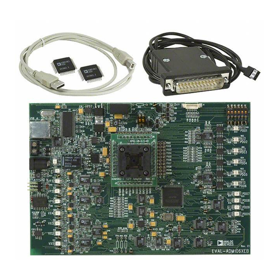
48-Lead TQFP SU-48 ADM1063ASUZ −40°C to +85°C 48-Lead TQFP SU-48 ADM1063ASUZ-REEL7 −40°C to +85°C 48-Lead TQFP SU-48 EVAL-ADM1063LFEB ADM1063 Evaluation Kit (LFCSP Version) EVAL-ADM1063TQEB ADM1063 Evaluation Kit (TQFP Version) Z = Pb-free part. Rev. 0 | Page 34 of 36... - Page 35 ADM1063 NOTES Rev. 0 | Page 35 of 36...
- Page 36 ADM1063 NOTES © 2005 Analog Devices, Inc. All rights reserved. Trademarks and registered trademarks are the property of their respective owners. D04632–0–4/05(0) Rev. 0 | Page 36 of 36...
Need help?
Do you have a question about the ADM1063 and is the answer not in the manual?
Questions and answers