Table of Contents
Advertisement
Quick Links
One Technology Way • P.O. Box 9106 • Norwood, MA 02062-9106, U.S.A. • Tel: 781.329.4700 • Fax: 781.461.3113 • www.analog.com
FEATURES
Simple power connection using USB connection and
on-board LDO voltage regulators
LDOs are easily bypassed for power measurements
AC-coupled differential SMA connectors
SMA connectors for
2 reference inputs
2 PLL status outputs
1 reference test input
2 VCXO interface inputs/outputs
Microsoft Windows®–based evaluation software
with simple graphical user interface
On-board PLL loop filter
Easy access to digital I/O and diagnostic signals
via I/O header
Status LEDs for diagnostic signals
USB computer interface
Software calculator provides flexibility, allowing programming
of almost any rational input/output frequency ratio
PLEASE SEE THE LAST PAGE FOR AN IMPORTANT
WARNING AND LEGAL TERMS AND CONDITIONS.
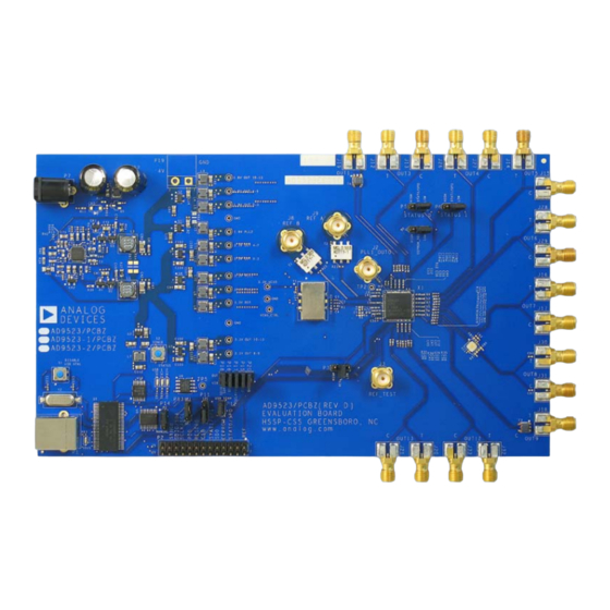
Evaluating the AD9523-1 Clock Generator
DIGITAL PICTURE OF EVALUATION BOARD
AD9523-1 Evaluation Board
Figure 1.
Rev. 0 | Page 1 of 16
Evaluation Board User Guide
GENERAL DESCRIPTION
This user guide describes the hardware and software of the
AD9523-1
evaluation boards. The evaluation board schematic
and PCB layout artwork can be found at www.analog.com.
The AD9523-1 is designed to support the clock requirements
for long-term evolution (LTE) and multicarrier GSM base station
designs. It relies on an external VCXO to provide the reference
jitter cleanup to achieve the restrictive low phase noise require-
ments necessary for acceptable data converter SNR performance.
The AD9523-1 evaluation board is a compact, easy-to-use plat-
form for evaluating all features of the AD9523-1. A 122.88 MHz
VCXO is mounted on the evaluation board to provide a complete
solution.
The input receivers are configured as differential but the evalua-
tion board has baluns to provide a single-ended input for easy
evaluation using common laboratory single-ended signal sources.
Output 8 is connected to an
ADCLK905
a way to evaluate an Analog Devices, Inc., buffer. Although the
ADCLK905 is a 1-to-1 buffer, the performance is similar to the
larger fanout buffer, for example, the 1-to-2 buffer, ADCLK925.
Output 1 and Output 9 are configured with baluns to provide a
single-ended output to drive most test equipment. Output 0 is
configured for differential zero delay operation.
UG-182
clock buffer to provide
Advertisement
Table of Contents

Related Manuals for Analog Devices UG-182


Summary of Contents for Analog Devices UG-182
-
Page 1: Features
ADCLK905 clock buffer to provide Software calculator provides flexibility, allowing programming a way to evaluate an Analog Devices, Inc., buffer. Although the of almost any rational input/output frequency ratio ADCLK905 is a 1-to-1 buffer, the performance is similar to the larger fanout buffer, for example, the 1-to-2 buffer, ADCLK925. -
Page 2: Table Of Contents
UG-182 Evaluation Board User Guide TABLE OF CONTENTS Features ....................1 Evaluation Board Software Operation..........6 General Description ................. 1 Menu Bar of Main Window ............7 Digital Picture of Evaluation Board ..........1 Using the Software to Control the Functional Blocks of ... -
Page 3: Evaluation Board Hardware
Evaluation Board User Guide UG-182 EVALUATION BOARD HARDWARE The following instructions are for setting up the physical SETTING UP THE SIGNAL CONNECTIONS connections to the AD9523-1 evaluation board. After setting up the power and PC connections, use the SETTING UP JUMPER CONNECTIONS... -
Page 4: Using I C Serial Port Mode
UG-182 Evaluation Board User Guide USING I C SERIAL PORT MODE To use the I2C serial Port mode, follow these steps: Power down the board and shut down the software. Set Jumpers P11 and P13 to the I2C position (see Figure 2). -
Page 5: Evaluation Board Software Setup
Double-click the Software folder, and then double-click AD9523-1Eval_Setup1.1.0.exe. Follow the installation instructions. The default location for the evaluation software is C:\Program Files\Analog Devices\AD9523-1 Eval Software\. Figure 4. Select USB Device Window If there are any updates to the evaluation software on a... -
Page 6: Evaluation Board Software Operation
UG-182 Evaluation Board User Guide EVALUATION BOARD SOFTWARE OPERATION The main window of the AD9523-1 evaluation board software When a subsection window closes after clicking OK, the comprises subsections that correspond to the major functional WRITE button under REGISTER W/R on the main window blocks of the AD9523-1 (see Figure 6). -
Page 7: Menu Bar Of Main Window
Evaluation Board User Guide UG-182 MENU BAR OF MAIN WINDOW File Menu The File menu allows you to load a previously saved AD9523-1 setup file or to save a new AD9523-1 setup file. A setup file (.stp) is a text file that contains the AD9523-1 register setup file, plus any evaluation board settings. -
Page 8: Using The Software To Control The Functional Blocks Of Ad9523-1
UG-182 Evaluation Board User Guide The Register Map Values window, accessed by selecting SYNC, PD (Power Down), and RESET Register Map Window from the View menu, allows you to read The SYNC, PD, and RESET buttons allow you to control the registers (see Figure 10). -
Page 9: Pll 2 Controls
Evaluation Board User Guide UG-182 Reference (REF) Divider Window The Charge Pump Setup window shown in Figure 15 is accessed by clicking the CHARGE PUMP box in Figure 12. This window is most often used to vary the charge pump current. -
Page 10: Channel Divider Window
UG-182 Evaluation Board User Guide Feedback (N) Divider Window CHANNEL DIVIDER WINDOW Figure 20. Channel Divider Window Figure 18. N Divider Window The channel divider window shown in Figure 20 is accessed by clicking the appropriate channel divider (see Figure 21) in the The N Divider window shown in Figure 18 is accessed by main window shown in Figure 6. -
Page 11: Output Driver Window
Evaluation Board User Guide UG-182 OUTPUT DRIVER WINDOW EEPROM CONTROL Figure 25. EEPROM Control Window The EEPROM Control window shown in Figure 25 is accessed by clicking the EEPROM button near the lower left quadrant of the main window. To store the current register settings of the AD9523-1 to the EEPROM, click the Program EEPROM button. -
Page 12: Using The Evaluation Board To Program An Ad9523-1 On A Customer Board
UG-182 Evaluation Board User Guide USING THE EVALUATION BOARD TO PROGRAM AN AD9523-1 ON A CUSTOMER BOARD This guide explains how to use an AD9523-1 evaluation board Click Reset Serial Port and then click Detect Current to program an AD9523-1 on a customer board via the I C inter- Configuration. -
Page 13: Quick Start Guide To The Ad9523-1
Evaluation Board User Guide UG-182 QUICK START GUIDE TO THE AD9523-1 The AD9523-1 can be initialized at startup from either the To load the provided setup file: EEPROM or from SPI settings. The AD9523-1 evaluation board Follow the instructions provided in the Evaluation Board ships with initial settings programmed in the EEPROM. - Page 14 UG-182 Evaluation Board User Guide NOTES Rev. 0 | Page 14 of 16...
- Page 15 Evaluation Board User Guide UG-182 NOTES Rev. 0 | Page 15 of 16...
- Page 16 By using the evaluation board discussed herein (together with any tools, components documentation or support materials, the “Evaluation Board”), you are agreeing to be bound by the terms and conditions set forth below (“Agreement”) unless you have purchased the Evaluation Board, in which case the Analog Devices Standard Terms and Conditions of Sale shall govern. Do not use the Evaluation Board until you have read and agreed to the Agreement.
Need help?
Do you have a question about the UG-182 and is the answer not in the manual?
Questions and answers