Table of Contents
Advertisement
Quick Links
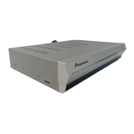
Digital Terrestrial Receiver
DBR-TF100
THIS MANUAL IS APPLICABLE TO THE FOLLOWING MODEL(S) AND TYPE(S).
Model
Type
DBR-TF100
NYXKEW
÷
When servicing the PCB Assy, handle with full care.
Refer to "7.4 CAUTION FOR PCB ASSY SERVICING" for details.
For details, refer to "Important symbols for good services".
PIONEER CORPORATION
PIONEER ELECTRONICS (USA) INC. P.O. Box 1760, Long Beach, CA 90801-1760, U.S.A.
PIONEER EUROPE NV Haven 1087, Keetberglaan 1, 9120 Melsele, Belgium
PIONEER ELECTRONICS ASIACENTRE PTE. LTD. 253 Alexandra Road, #04-01, Singapore 159936
PIONEER CORPORATION 2004
Power Requirement
AC220-230V
4-1, Meguro 1-chome, Meguro-ku, Tokyo 153-8654, Japan
DBR-TF100
T-ZZK MAY 2004 printed in Japan
ORDER NO.
ARP3204
Remarks
Advertisement
Table of Contents

Related Manuals for Pioneer DBR-TF100


Summary of Contents for Pioneer DBR-TF100
- Page 1 PIONEER CORPORATION 4-1, Meguro 1-chome, Meguro-ku, Tokyo 153-8654, Japan PIONEER ELECTRONICS (USA) INC. P.O. Box 1760, Long Beach, CA 90801-1760, U.S.A. PIONEER EUROPE NV Haven 1087, Keetberglaan 1, 9120 Melsele, Belgium PIONEER ELECTRONICS ASIACENTRE PTE. LTD. 253 Alexandra Road, #04-01, Singapore 159936...
-
Page 2: Safety Information
For the latest information, always consult the current PIONEER Service Manual. A subscription to, or additional copies Also test with plug reversed of, PIONEER Service Manual may be obtained at a (Using AC adapter Earth nominal charge from PIONEER. plug as required) -
Page 3: Table Of Contents
6. ADJUSTMENT ..............................31 7. GENERAL INFORMATION ..........................32 7.1 DIAGNOSIS..............................32 7.1.1 CHECK MODE ...........................32 7.1.2 TROUBLE SHOOTING........................39 7.2 IC ................................45 7.3 MOUNTING CONDITION FOR BGA......................59 7.4 CAUTION FOR PCB ASSY SERVICING ....................61 7.5 TEST POINTS INSTRUCTION .........................62 8. PANEL FACILITIES ............................65 DBR-TF100... -
Page 4: Specifications
& Mains lead (ADG1154) Connects the DTR SCART socket to the TV SCART socket. (TV SCART sockets are usually labelled EXT or AV.) & Instruction manuals & Warranty card This is provided separately. Plug it into the mains power supply. DBR-TF100... -
Page 5: Exploded Views And Parts List
• • • • • • Card Board Insert XHB1006 Remote Control XXD1003 Packing Case XHD1028 NSP 4 Battery(AA/R06) VEM1017 Instruction Manual XRB1016 Aerial/RF Lead BDE1064 (English/French/Italian) SCART Lead BDH1039 Instruction Manual XRB1015 (German/Spanish) NSP 8 Warranty Card XRY1008 Sheet AHG1153 DBR-TF100... -
Page 6: Exterior Section
2.2 EXTERIOR SECTION IC3002 P301 (Side-B) DBR-TF100... - Page 7 XNB1004 Tuner Spring XBH1003 • • • • • • Spacer XEC1001 Light Shield XEC1002 Ground Plate BBK1004 Front Panel Assy XWX1007 Foot XMR1006 Bonnet XNE1006 Protect Label BAX1302 NSP 17 Bar Code Label XAL1015 Screw BBZ30P060FZK Screw BBZ30P080FZK DBR-TF100...
-
Page 8: Block Diagram And Schematic Diagram
3.1 BLOCK DIAGRAM MAIN ASSY M1000 IC1001 IC3000 COFDM SDRAM STV0360 64Mbit Tuner Murata IC1002 RF Modulator IC2000 STi5517 MC44BS373 Q1200 Q1201 MPEG A / V Demux Decoder Card IF UART UART Serial IF RS232 Tuner I2C PAL, Audio DBR-TF100... - Page 9 SDRAM 16Mbit 64Mbit PAL, SVHS, RGB, Audio PAL, Audio CN4000 IC4003 PAL, SVHS, RGB PAL / SECAM AV Switch Encoder STV6413 PAL, SVHS, Audio PAL, SVHS / RGB, CN4001 Audio I2C SPDIF JA4000 SPDIF out (optical) IC4002 Audio L+R DBR-TF100...
-
Page 10: Overall Wiring Connection Diagram
3.2 OVERALL WIRING CONNECTION DIAGRAM 1/5 - MAIN ASSY (XWE1011) DBR-TF100... - Page 11 • The > mark found on some component parts indicates the importance of the safety factor of the part. Therefore, when replacing, be sure to use parts of identical designation. • : The power supply is shown with the marked box. POWER ASSY (XXF1004) DBR-TF100...
-
Page 12: Main Assy (1/5)
3.3 MAIN ASSY (1/5) MAIN ASSY (XWE1011) Tuner GND1 INPUT1 OUTPUT1 INPUT2 OUTPUT2 GND2 SAW Filter RF Amp DBR-TF100... - Page 13 Modulator IC COFDM LINK IC DBR-TF100...
-
Page 14: Main Assy (2/5)
3.4 MAIN ASSY (2/5) Prog. Transport IC Reset IC 11 12 DBR-TF100... - Page 15 MAIN ASSY (XWE1011) DBR-TF100...
-
Page 16: Main Assy (3/5)
3.5 MAIN ASSY (3/5) SDRAM(64MBit) MAIN ASSY (XWE1011) DBR-TF100... - Page 17 FLASH(16MBit) SDRAM(64MBit) XYW1002 DBR-TF100...
-
Page 18: Main Assy (4/5)
3.6 MAIN ASSY (4/5) DBR-TF100... - Page 19 MAIN ASSY (XWE1011) DBR-TF100...
-
Page 20: Main Assy (5/5)
3.7 MAIN ASSY (5/5) Remote Sensor Unit 1/5,2/5 1/5,4/5 1/5,4/5 2/5,4/5 DBR-TF100... - Page 21 MAIN ASSY (XWE1011) DBR-TF100...
-
Page 22: Power Assy
3.8 POWER ASSY POWER ASSY (XXF1004) LIVE NEUTRAL DBR-TF100... - Page 23 Note : No individual parts replacement for repair except F101 and P301 is accepted by Model Supplier due to the safety reasons. > (1.25A) • NOTE FOR FUSE REPLACEMENT CAUTION - FOR CONTINUED PROTECTION AGAINST RISK OF FIRE. REPLACE WITH SAME TYPE AND RATINGS ONLY. DBR-TF100...
-
Page 24: Waveforms
V: 500mV/div. H: 20.0nsec/div. V: 2.0V/div. H: 100nsec/div. V: 1.0V/div. H: 20.0nsec/div. V: 1.0V/div. H: 100nsec/div. IC2001-pin 10 (27M) CS for IC3000 - (VSD_CS) CK1003 - (LOCK) V: 1.0V/div. H: 10.0nsec/div. V: 2.0V/div. H: 20.0nsec/div. V: 1.0V/div. H: 20.0nsec/div. DBR-TF100... - Page 25 V: 1.0V/div. H: 10.0nsec/div. V: 1.0V/div. H: 200µsec/div. CS for IC3003 - (SD_CS) CK4004 - (A_L2) V: 1.0V/div. H: 4.0nsec/div. V: 1.0V/div. H: 200µsec/div. CK4006 - (A_R2) Clock for IC3003 - SD_CLK) V: 1.0V/div. H: 200µsec/div. V: 1.0V/div. H: 4.0nsec/div. DBR-TF100...
-
Page 26: Pcb Connection Diagram
4. PCB CONNECTION DIAGRAM 4.1 MAIN ASSY SIDE A MAIN ASSY Q1003 Q1002 Q1004 IC4002 Q4004 Q4003 Q1000 Q1001 IC3000 Q1201 Q1200 IC1000 IC2000 IC1001 IC2001 IC3002 IC3003 DBR-TF100... - Page 27 For further information for respective destinations, be sure to check with the schematic diagram. 4. View point of PCB diagrams. Capacitor Connector (XNP1011-A) SIDE A Q4004 Q4003 Q4006 Q4005 IC4001 IC4003 Q2001 Q4000 Q5005 Q5008 IC2003 IC2008 IC3003 Q5003 Q5101 Q5001 SIDE B P.C.Board Chip Part DBR-TF100...
- Page 28 SIDE B MAIN ASSY DBR-TF100...
- Page 29 SIDE B (XNP1011-A) DBR-TF100...
-
Page 30: Pcb Parts List
CCSRCH471J50 C1009,C1010,C1022 CEHAT471M10 C2026 CEHAT101M10 C1061 CKSRYB102K50 C2024,C2025 CEHAT101M16 C1000,C1002,C1005,C1013 CKSRYB103K50 C2006,C2012,C2015,C2016 CKSRYB102K50 C1033,C1034,C1038,C1060,C1062 CKSRYB103K50 C2009 CKSRYB105K10 C1064,C1065 CKSRYB103K50 C2000 CKSRYB471K50 C1007,C1008,C1014,C1021 CKSRYB104K16 C2001,C2003,C2005,C2008 CKSRYF104Z16 C1023-C1028,C1030-C1032,C1035 CKSRYB104K16 C2013,C2014,C2017-C2020 CKSRYF104Z16 C1039,C1044-C1047,C1049 CKSRYB104K16 C2028-C2031,C2033-C2035 CKSRYF104Z16 C1053,C1054,C1057,C1066,C1079 CKSRYB104K16 C2037-C2039,C2041-C2043 CKSRYF104Z16 C1083 CKSRYB104K16 DBR-TF100... -
Page 31: Adjustment
CEHAT101M16 Refer to “2.2 EXTERIOR SECTION” for the spec of F101. C4045 CEHAT1R0M50 C4015,C4035 CEHAT221M10 C4053-C4059,C4061,C4200 CKSRYB102K50 6. ADJUSTMENT C4012 CKSRYB103K50 C4005-C4007,C4009-C4011,C4026 CKSRYB104K16 There is no information to be shown in this chapter. C4036,C4044,C4047,C4051 CKSRYB104K16 C4020,C4021,C4032,C4034,C4046 CKSRYB105K10 C4048-C4050 CKSRYB105K10 DBR-TF100... -
Page 32: General Information
7.1 DIAGNOSIS 7.1.1 CHECK MODE 1. Inspection Software Mode The DBR-TF100 test software is resident in the flash. ¶ How to enter Inspection Software Mode: 1. Connect the serial debug PCB (GGF1348) to the IRD (see diagram below). 2. Switch on the IRD. - Page 33 PC Operation Environment DOS/V machine OS: MS-DOS Execution Program: GA0015B.exe (Order Code PEE1034) Selecting the required model When GA0015B.exe is started the following screen initial screen is displayed. Press the Return Key to select DBR-TF100. The following screen will be displayed. DBR-TF100...
- Page 34 Press " y " to overwrite the existing " make step_file ". The following menu of options is displayed. Use the cursor keys to move around the menu and press enter to add steps. When all required steps are added press f10 to return to the MAIN MENU screen. DBR-TF100...
- Page 35 Reserved Reserved Reserved Reserved ∗1 Check VCXO Change the VCXO frequency between max and min levels ∗2 Check Slow_SW 4:3 (12V) Set the slow switch level to 12V Reserved ∗3 Check SUM:Boot Check that is used only in production DBR-TF100...
- Page 36 (f1~f4) Set Tuning Parameter 1~4: Used to set the parameters of the received signal. After completion of settings, the data is transmitted to the IRD by pressing the " f9 " key. (f5) Set the state of the IRD: This is used to set slow switch level, etc. DBR-TF100...
- Page 37 (f9) Set the audio level: This is used to adjust the audio level. 0 is maximum level and 9 is minimum level. After completion of settings, the data is transmitted to the IRD by pressing the " f9 " key. DBR-TF100...
- Page 38 Interruption of resident software download should not cause a problem at any stage. Examples of terminal display: download –wbo boot_64.bin –port com download boot software contained in boot_64.bin via COM download- wrs fta.bin download resident software contained in fta. bin bia COM DBR-TF100...
-
Page 39: Trouble Shooting
Is there a Is there OSD? Enter Section(3) picture? Enter FE troubleshooting section(4) Is there Enter SMI troubleshooting macroblock section(3) and FE on display? troubleshooting (4a) Is there Enter Audio sound? troubleshooting section(4) RF output Enter FE Section(4a) STB working OK DBR-TF100... - Page 40 IC3001 Is Address and Data OK? Check SD_CLK Check Address and Data 90MHz lines inc. Resistors Repair Check F_OE Check SDRAM Replace IC2000 Control lines on power cycle Repair Check around resistors and ferrite beads Change SDRAM DBR-TF100...
- Page 41 X1001 Replace IC1002 Replace Q4000 Check 4MHz X1001 Check I2C on Check R1042/R1043 IC1002 pin 1 and 2 Check I2C on R2047 and R2048 Change IC1002 Check picture on Change M1000 RF Modulator Return to MAIN Assy Flow chart DBR-TF100...
- Page 42 Trace back to IC1001 pin12 low IC2000 10ms on power up Trace back to Check I2C IC2000 pin 18 and 19 R2045 & R2046 of IC1001 Check error pin40 (R1051), Test point Replace IC2000 AVDAT0-7, AVVALID, AVFSTART AVCLK Replace IC1001 DBR-TF100...
- Page 43 C → 8 VCR_CVBS/Y → 48,VCR_C → 46 R → 10 G → 12 Replace IC4003 B → 14 Check for video signal at Omega Replace filter components side of filters? (C4005/6/7, C4009/10/11) Check R2054/ Omega NG, replace R2055 Replace DBR-TF100...
- Page 44 From Main flowchart Switch antenna power ON in software Check around 3.3V at Antenna Disconnect Q1003/Q1002/R1063 base of power external antenna. Repair as necessary. Q1004? Antenna Return to main Omega or Q1004 NG. power flowchart Check and replace. Replace Tuner DBR-TF100...
- Page 45 • The information shown in the list is basic information and may not correspond exactly to that shown in the schematic diagrams. List of IC BD4720G, uPC3221GV, MC44BS373CAD, STV6413D, STV0360, STI5517AWA BD4720G (MAIN ASSY : IC2003) • Reset IC Pin Arrangement Vout N.C. Block Diagram Vout Vref DBR-TF100...
- Page 46 OUTPUT1 INPUT2 OUTPUT2 GND2 AGC CONTROL Pin Function Pin Name Function Power Supply pin. INPUT1 Signal input pins to AGC amplifier. INPUT2 Gain control pin. GND2 Ground pin. OUTPUT2 Signal output pins of video amplifier. OUTPUT1 GND1 Ground pin. DBR-TF100...
- Page 47 (only in MLF 20) BUS SECTION VCO and PLL SECTION VHF Dividers (only in MLF 20) UHF OSC High Speed C Bus Prescaler/8 Receiver Prog Phase Ref Divider 4MHz Divider Comp /128 C BUS 31.25KHz VCCD GNDD PLLFLT XTAL DBR-TF100...
- Page 48 Mute ROUT_CINCH LIN_TV VCR Switch 0/6 dB LOUT_CINCH 0/6/9 dB RIN_ENC LIN_ENC RIN_TV LIN_VCR LIN_VCR -62 dB 0/6 dB LIN_TV LOUT_TV Stereo/ Mono ROUT_TV RIN_ENC RIN_VCR RIN_VCR -62 dB 0/6 dB RIN_TV Mute I≤ C Bus Decoder TV Switch DBR-TF100...
- Page 49 Audio Right Output to TV SCART LOUT_TV Audio Left Output to TV SCART Not connected Not connected Not connected VCCB5 Video Output Buffer Supply Pin BOUT_TV Blue Output to TV SCART VCCB4 Video Output Buffer Supply Pin GOUT_TV Green Output to TV SCART DBR-TF100...
- Page 50 SLB_TV Slow Blanking Input/Output from TV SCART R/CIN_VCR Red Input (or C Input) from VCR SCART SLB_VCR Slow Blanking Input/Output from VCR SCART GIN_VCR Green Input from VCR SCART VCC12 +12 V Supply BIN_VCR Blue Input from VCR SCART DBR-TF100...
- Page 51 Viterbi I≤ C decoder monitoring SCLT Interface De-interleaver De-interleaver SDAT Constellation display Control Reed- Solomon General decoder Lock purpose indicators Descrambler I/Os display LOCK/OP1 on OP1/OP2 and lock indicators LOCK/OP2 TS output DP, D0 to D7, CLK_OUT STR_OUT (ERROR) DBR-TF100...
- Page 52 Chip select LSB Chip select MSB Power supply Pin Name Function − 13, 28, 39, 57 VDD Digital core supply − 22, 35, 44, 52 VDD_3.3 Digital I/O supply 15, 24, 30, 37, − 41, 46, 54, 56, Ground DBR-TF100...
- Page 53 STI5517AWA (MAIN ASSY : IC2000) • Prog. Transport IC Pin Arragement DBR-TF100...
- Page 54 8K SRAM DENC 8K Dcache FIFOs interface STBus S/PDIF Audio 2x i/f MAFE Parallel MMDSP SmCard Tx/Rx interface I/O 6x cap/comp TSMUX FDMA Audio UARTs SSCs DACs TSIN1 TSIN2L LLI in/out Analog audio 2x serial/parallel out L/R TS input DBR-TF100...
- Page 55 Function CLK27MA Selectable input clock to PLL or for x1 mode CLKSPEEDSEL PLL speed select AUXCLKOUT Auxiliary clock for general use NOTRESET System reset NOTWDOGRSTOUT Internal watchdog timer reset. a : 5 V tolerant b : 1.8 V tolerant DBR-TF100...
- Page 56 : 5 V tolerant b : Input for TSIN2L and TSIN3 (1394). c : Output as TSIN1 byte clock signal. d : H25, H24, H23, J26, J24, K26, K25 and K24 e : TSIN2LDATA7 is used for data input in serial mode. DBR-TF100...
- Page 57 Audio/video core SDRAM data bus upper byte enable a : AC24, AC23, AD26, AD25, AD24, AD23, AE26, AE25, AE24, AE23, AF26, AF25, AF24 and AF23. b : V24, W26, W25, W24, W23, Y26, Y25, Y24, AA26, AA25, AA24, AB26, AB25, AB24, AC26 and AC25. DBR-TF100...
- Page 58 BOUT AD12 Blue output COUT Chroma output CVOUT AD10 Composite video output YOUT AE10 Luma output Analog video DAC pins Pin Name Location Function NOTHSYNC AE20 I/O Horizontal sync EVENNOTODDA AF20 I/O Vertical sync a : 5 V tolerant DBR-TF100...
-
Page 59: Mounting Condition For Bga
Max. Temperature Ramp-Down Rate Ramp-Up Rate (245 +/-5deg.C) 6deg.C/sec.Max. 3deg.C/sec.Max. 240deg.C 220d eg.C 100 to180 deg.C 30sec.MAX 150sec.Max 90sec.MAX Time (Seconds) Figure 1: Recommended temperature profile (conforming to JEDEC-STD-020) Time from Room Temperature to Peak 240 to 360 sec. DBR-TF100... - Page 60 1.3 above. If you remove the product using hot air in a status where the resin has absorbed moisture, heat stress may cause package cracking or adhesion degradation of the resin, and the actual reason for nonconformity may not found easily. DBR-TF100...
-
Page 61: Caution For Pcb Assy Servicing
- Be carefull not to short the 5V supply lines. If this occurs, the IC protector P301 on the POWER Assy will blow. Ground Plate (Copper Clips) Fingers Scart Connector Fig.1 Scart socket copper clips Fig.2 Tuner Bottom Can Solder Point Solder Point Fig.3 Tuner Bottom Can DBR-TF100... -
Page 62: Test Points Instruction
MAIN_1/5 TS1_1 AVDAT1 Data 1 MAIN_1/5 TS1_2 AVDAT2 Data 2 MAIN_1/5 TS1_3 AVDAT3 Data 3 MAIN_1/5 TS1_4 AVDAT4 Data 4 TS1_5 AVDAT5 Data 5 MAIN_1/5 MAIN_1/5 TS1_6 AVDAT6 Data 6 MAIN_1/5 TS1_7 AVDAT7 Data 7 MAIN_1/5 TS1_10 AVFSTART Start DBR-TF100... - Page 63 RAS for IC3000 (Video SDRAM) MAIN_3/5 SD_XCAS VSD_CAS CAS for IC3000 MAIN_3/5 SD_XWE VSD_WE Write enable for IC3000 MAIN_3/5 SD_XCS0 VSD_CS Chip select for IC3000 (5) Other Points (Resistor) Signal Name Indicate Description Wave Form No. SD_CLK MAIN_3/5 VSD_CLK Clock for IC3000 DBR-TF100...
- Page 64 Fig.1 Test Points SIDE A DBR-TF100...
-
Page 65: Panel Facilities
2 SCART socket for VCR 6 VHF and UHF aerial input, +5V to external antenna 3 SCART socket for TV 4 Optical digital audio output socket 1. SCART: Euroconnector 2. VHF: Very High Frequency 3. UHF: Ultra High Frequency DBR-TF100... - Page 66 0 Refer to Setting TV codes on the right. This remote can directly control the TVs of major manufacturers. At the time of ship- ment the remote is preset to operate Pioneer TVs. - SUBTITLE button Press to display subtitles. = WIDE button Press to switch between wide-screen viewing modes.
Need help?
Do you have a question about the DBR-TF100 and is the answer not in the manual?
Questions and answers