Table of Contents
Advertisement
Quick Links
RTKA271082DE0000BU
The RTKA271082DE0000BU evaluates the
performance of the
RAA271082
with three synchronous buck regulators and one low
dropout linear regulator. The evaluation board is
intended for use in point-of-load automotive
applications, including camera systems, with 4.5V to
42V input supply range.
In addition to four output voltages, the evaluation
board also contains an I
indicator, and a general purpose I/O (GPIO) signal.
The RAA271082 is offered in a 4mm×4mm 24-lead
Step Cut QFN (SCQFN) package with an exposed
pad. The RAA271082 is qualified to AEC-Q100,
Grade1.
Enable From System,
or EN tied to VIN1 pin
VIN
(4-42V, 45V max)
LV Enable From System
or EN_LV tied to BYP
_
4.7µF
BYP
2
I
C Serial
Interface
R33UZ0006EU0100 Rev.1.00
Jul 25, 2022
Automotive PMIC
2
C interface, a RSTB status
EN
VIN1
EN_LV
BYP
RAA271082
CFG1
SDA
SCL
GPIO
RSTB
Figure 1. Block Diagram
Evaluation Board Manual
Features
▪ V
operating range from 4.0 to 42V
IN
▪ Start range 4.5 to 42V
▪ Three synchronous bucks with internal
compensation and one LDO
▪ Fixed Frequency 2.2MHz
▪ Over-temperature, overcurrent, overvoltage and
negative overcurrent protection
Specifications
▪ V
range: 4V to 42V
IN
▪ V
range 2.8V to 5.05V, up to 1A
OUT1
▪ V
range 0.85V to 3.3V, up to 1A
OUT2
▪ V
range 0.85V to 3.3V, up to 1A
OUT3
▪ LDO4 range 2.87V to 3.4V, up to 300mA
2
▪ I
C interface
▪ RSTB and GPIO signals
0.22µF
BOOT1
4.7µH
PHASE1
PGND1
FB1
LDOIN4
0.1µF
LDOOUT4
1µF
VIN2/3
0.1µF
1.5µH
PHASE2
FB2
PGND2/3
1.5µH
PHASE3
FB3
VOUT1
3.8V at 1A
(2.8V – 5.05V)
10µF
LDOOUT4
3.3V at 300mA
(2.7V – 3.4V)
VOUT2
1.8V at 1A
(0.85V - 3.3V)
2x10µF
VOUT3
1.2V at 1A
(0.85V - 3.3V)
2x10µF
© 2022 Renesas Electronics
Page 1
Advertisement
Table of Contents

Subscribe to Our Youtube Channel
Related Manuals for Renesas RTKA271082DE0000BU


Summary of Contents for Renesas RTKA271082DE0000BU
- Page 1 Evaluation Board Manual RTKA271082DE0000BU Features The RTKA271082DE0000BU evaluates the performance of the RAA271082 Automotive PMIC ▪ V operating range from 4.0 to 42V with three synchronous buck regulators and one low ▪ Start range 4.5 to 42V dropout linear regulator. The evaluation board is ▪...
-
Page 2: Table Of Contents
RTKA271082DE0000BU Evaluation Board Manual Contents Functional Description ..............3 Manual Output Control using EN and EN_LV . -
Page 3: Functional Description
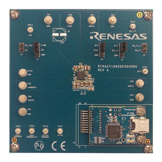
RTKA271082DE0000BU Evaluation Board Manual Functional Description The evaluation board with connections, headers, and test points is shown in Figure J1: 3-Pin Header J3: 3-Pin Header for for Manual EN Control VIN1 Input Vout1 Output Manual EN_LV Control (GND) (GND) TP14:... -
Page 4: Manual Output Control Using En And En_Lv
RTKA271082DE0000BU Evaluation Board Manual Manual Output Control using EN and EN_LV For manual control of EN, install a jumper on J1 and ensure that J2 jumper is not installed.. The upper position of J1 connects EN to the VIN1 supply and enables the IC. The lower position connects EN to GND and disables the IC. -
Page 5: Input And Output Connections And Test Points
RTKA271082DE0000BU Evaluation Board Manual 1.3.1 Input and Output Connections and Test Points The input and output connections are shown in Figure 1 Table 1 Table 1. (+) Test Point GND Test Point Default Value (V) VIN1 (input) 12 (4V to 42V, 4.5V to start) - Page 6 RTKA271082DE0000BU Evaluation Board Manual When powered up, the GUI should initially appear as shown in Figure Configure Tab is Active Tab Select Dongle Found Counter Output Voltage VIN ULVO Output Voltage Select Select Device ID Output OV Information Threshold Output UV...
-
Page 7: Changing Programming Options
RTKA271082DE0000BU Evaluation Board Manual ▪ VIN UVLO drop-down: Selects the V UVLO threshold. ▪ Device ID information: Reads the device ID and silicon revision. ▪ EN control: Controls the Buck1 output and Standby operation. ▪ EN_LV control: Controls the LV outputs (Buck2, Buck3, LDO4). -
Page 8: Fault Status Tab
RTKA271082DE0000BU Evaluation Board Manual Note: While options can be selected, the accuracy of the selected options may be slightly outside the datasheet specifications. Datasheet accuracy limits are assured only for the factory-programmed settings. As an example, if Vout1 is selected to the default value of 3.8V, the output value is finely adjusted at the factory for Vout1 set to 3.8V. -
Page 9: Displaying Detected Faults
RTKA271082DE0000BU Evaluation Board Manual does not show drop-downs for NOC (Negative Overcurrent) fault or for Severe UV fault; these faults cannot be detected. At the bottom of the Fault Status tab are fault indicators for the Watchdog Timer (WWDT), DAC Compare faults, Sequence faults, I2C CRC faults, and CRC Recheck faults. -
Page 10: Fault Response Mask Tab
RTKA271082DE0000BU Evaluation Board Manual In the example, the CRC Recheck fault is detected. In this case, there is no button to clear all these faults at once; each fault must be cleared individually using the drop-downs. Figure 7. Fault Status Tab – WWDT and Other Faults Figure 7, the CRC Recheck fault (far right) shows a fault detected. -
Page 11: Fault To Gpio Control Tab
RTKA271082DE0000BU Evaluation Board Manual Each of the output-related fault responses can be enabled or disabled by selecting the drop-down. Selecting no response to fault causes the device to not respond (not shut down any outputs) if the fault is detected. -
Page 12: Gpio Pin Tab
RTKA271082DE0000BU Evaluation Board Manual All drop-downs on this tab are configured to display ignore GPIO on fault or assert GPIO pin low on fault. Use the drop-downs to select which, if any, faults cause the GPIO pin to assert low when the fault is detected. These selections can be made whenever EN is at Standby or On and have no effect on the ReCal CRC operation. -
Page 13: Rstb Pin / Wwdt Tab
RTKA271082DE0000BU Evaluation Board Manual ▪ GPIO Write Data: If GPIO is selected as a logic output, this bit dictates which logic state (1 or 0) is sent to the pin. ▪ GPIO Pin function select: For all options in this selection (see... - Page 14 RTKA271082DE0000BU Evaluation Board Manual ▪ WWDT lockout, a feature that locks the WWDT settings and prevents any future changes. ▪ Which WWDT faults are sent to the RSTB pin as fault indicators. ▪ If a WWDT fault occurs, the response can be to shut down all outputs or shut down only LV outputs.
- Page 15 RTKA271082DE0000BU Evaluation Board Manual The explanations for the drop-downs in Figure 11 are shown below. From the right side: ▪ Power Good selections for RSTB. The default setting for RSTB is that any output below its UV threshold will generate a RSTB low fault indication. This opt_pg_rstb drop-down allows RSTB to ignore some outputs based on drop-down selection.
-
Page 16: Misc Tab
RTKA271082DE0000BU Evaluation Board Manual Misc Tab The Misc tab shown in Figure 12 is selected by clicking the Misc tab in the tab row. This tab controls miscellaneous options that are found in registers 0x7B, 0x7C, and 0x7D of the RAA271082. Note: All options on this tab are CRC checked and therefore can be changed only when the device is in Standby mode. -
Page 17: Misc1 Options - Register 0X7B
RTKA271082DE0000BU Evaluation Board Manual 2.7.1 Misc1 Options – Register 0x7B Misc1 options are shown in Figure 12 in the Misc1 Options box at the top. ▪ Hiccup/latchoff options: The device has four selections for hiccup/shutdown for response per register 0x7B bits 7,6. -
Page 18: Misc3 Options - Register 0X7D
RTKA271082DE0000BU Evaluation Board Manual 2.7.3 Misc3 Options – Register 0x7D Misc3 options are shown in Figure 12, in the Misc3 Options box at the bottom right side. ▪ Optional Buck3 OC: This option selections different Overcurrent (OC) levels for Buck3. The default value is 1.20A, with options of 0.96A and 1.56A. -
Page 19: Rea Dongle Tab
RTKA271082DE0000BU Evaluation Board Manual REA Dongle tab The REA Dongle tab shown in Figure 12 below is selected by clicking the REA Dongle tab in the tab row. This tab can be used to perform direct read and write operations on specific registers. - Page 20 RTKA271082DE0000BU Evaluation Board Manual The Log tab also contains a Clear Log button which clears away all previous read/write information. This is helpful in tracking individual register operations. Running log of read/write transactions between the GUI and the RAA271082. Clear Log button: Click this to clear all Log entries.
-
Page 21: Board Design
RTKA271082DE0000BU Evaluation Board Manual Board Design Figure 16. RTKA271082DE0000BU Evaluation Board (Top) Figure 17. RTKA271082DE0000BU Evaluation Board (Bottom) R33UZ0006EU0100 Rev.1.00 Page 21 Jul 25, 2022... -
Page 22: Layout Guidelines
Route the trace so that it avoids passing underneath the inductors L2, L3, or L1, and also avoids passing underneath under the PHASE signals or pins. Renesas recommends routing the trace on an inner layer, going around COUT3, and then routing to Pin 22. VOUT2 (Buck2 output) and the FB2 pin are shown in... - Page 23 RTKA271082DE0000BU Evaluation Board Manual ▪ Connect all the grounds pins (Pins 10, 11, and 22) and the thermal PAD (Pin 25) together using a single wide copper pad under the IC. Connect this copper pad to the ground plane using multiple vias, to provide a low-impedance path to the ground plane and also to provide heatsinking through the PCB copper.
-
Page 24: Schematic Diagram
RTKA271082DE0000BU Evaluation Board Manual Schematic Diagram VOUT1 VOUT2 VIN1 VOUT3 LDOOUT4 Spare output capacitors Digital signal probes I2C Dongle Connector Figure 19. RTKA271082DE0000BU Schematic R33UZ0006EU0100 Rev.1.00 Page 24 Jul 25, 2022... -
Page 25: Bill Of Materials
RTKA271082DE0000BU Evaluation Board Manual Bill of Materials Reference Designator Description Manufacturer Manufacturer Part CAP-AEC-Q200, SMD, 0402, 0.22µF, Murata GCM155R71C224KE02D 16V, 10%, X7R, ROHS CAP-AEC-Q200, SMD, 0402, 0.1µF, C27, C28 Murata GCM155R71H104KE02D 50V, 10%, X7R, ROHS CAP-AEC-Q200, SMD, 0603, 1µF, 25V,... -
Page 26: Board Layout
RTKA271082DE0000BU Evaluation Board Manual Reference Designator Description Manufacturer Manufacturer Part J5-SEE ASSEMBLY NUT, 4-40, HEX, 18-8 STAINLESS MCMASTER- 91841A005 INSTRUCTIONS STEEL, ROHS CARR J5-SEE ASSEMBLY SCREW, 4-40×1/2in, PHILLIPS PAN, Building PMSSS 440 0050 PH INSTRUCTIONS STAINLESS, ROHS Fasteners SCREW, 4-40×1/4in, PHILLIPS,... - Page 27 RTKA271082DE0000BU Evaluation Board Manual Figure 22. Top Layer Figure 23. Layer 2 Figure 24. Layer 3 Figure 25. Bottom Layer R33UZ0006EU0100 Rev.1.00 Page 27 Jul 25, 2022...
-
Page 28: Typical Performance Graphs
RTKA271082DE0000BU Evaluation Board Manual Figure 26. Bottom Layer Copper and Silkscreen Figure 27. Bottom Layer Silkscreen Typical Performance Graphs VOUT1 = 3.3V VIN1 = 9V VOUT1 = 3.6V VIN1 = 12V VOUT1 = 3.8V VIN1 = 15V VOUT1 = 5.0V... - Page 29 RTKA271082DE0000BU Evaluation Board Manual ▪ VOUT1 only on VOUT1 = 3.6V VOUT1 = 3.8V VOUT1-4 on VOUT1 = 5.0V 0.00 0.05 0.10 0.15 0.20 0.25 0.30 LDO4 Load (A) Figure 32. V to LDO4 = 3.3V, Efficiency vs Load Figure 33. V...
-
Page 30: Ordering Information
RTKA271082DE0000BU Evaluation Board Manual Ordering Information Part Number Description RTKA271082DE0000BU RAA271082 Evaluation board Revision History Revision Date Description 1.00 Jul 25, 2022 Initial release R33UZ0006EU0100 Rev.1.00 Page 30 Jul 25, 2022... - Page 31 Renesas Electronics disclaims any and all liability for any damages or losses incurred by you or any third parties arising from the use of any Renesas Electronics product that is inconsistent with any Renesas Electronics data sheet, user’s manual or other Renesas Electronics document.
- Page 32 Mouser Electronics Authorized Distributor Click to View Pricing, Inventory, Delivery & Lifecycle Information: Renesas Electronics RTKA271082DE0000BU...
Need help?
Do you have a question about the RTKA271082DE0000BU and is the answer not in the manual?
Questions and answers