Table of Contents
Advertisement
Quick Links
RTKA214023DE0000BU
The RTKA214023DE0000BU evaluation board
provides a simple platform to evaluate the
RAA214023. It contains all the important circuitry
needed to characterize critical performance
parameters.
The RAA214023 is a low noise, high PSRR, low
dropout voltage regulator. It accepts a input voltage
range of 2.7V to 5.5V, and the output voltage can be
programmed from 0.8V to 3.95V by means of voltage
setting pins. To extend the output voltage range up to
5.5V-V
, an external resistor divider feedback
DROPOUT
network can be used. The device can source a load
current of up to 2A and has an output voltage
accuracy of ±1.75% over line, load, and temperature.
V
OUT
3.3V,
I
OUT ( MAX)
2A
C6
C5
0.1µF
22µF
V
PG
R16UZ0020EU0100 Rev.1.00
Sep 16, 2021
R3
OUT
10kΩ
SNS
FB
PG
50mV
Figure 1. Block Diagram
Evaluation Board Manual
Features
▪ Input Voltage Range: 2.7V to 5.5V
▪ Voltage Set Pins easily programmed with JP1: 0.8V
to 3.95V
▪ Switch between Voltage Set pins or Eternal
Resistor Divider using jumper JP_FB
▪ Convenient shutdown mode function using Jumper
JP_EN
▪ Power good (PG) indication test point
Specifications
This board has been optimized for the following
operating conditions:
▪ V
range from 2.7V to 5.5V
IN
▪ V
adjustable from 0.8V to 3.95V with Voltage
OUT
Set Pins
▪ V
adjustable from 0.8V up to 5.5V - V
OUT
with External Resistor Divider
▪ Low dropout: 420mV at 2A and VIN= 3.3V (typical)
▪ High PSRR for V
• 100kHz: 62dB at 2A and 85dB at 500mA
• 1MHz: 51dB at 2A and 60dB at 500mA
IN
EN
RAA214023
CSET
NC
1.6V
= 1.7V:
HEADROOM
2.7V – 5.5V
R1
10kΩ
C3
C2
0.1µF
10µF
C4
1µF
© 2021 Renesas Electronics
DROPOUT
V
IN
Page 1
Advertisement
Table of Contents

Subscribe to Our Youtube Channel
Related Manuals for Renesas RTKA214023DE0000BU


Summary of Contents for Renesas RTKA214023DE0000BU
- Page 1 Evaluation Board Manual RTKA214023DE0000BU Features The RTKA214023DE0000BU evaluation board provides a simple platform to evaluate the ▪ Input Voltage Range: 2.7V to 5.5V RAA214023. It contains all the important circuitry ▪ Voltage Set Pins easily programmed with JP1: 0.8V needed to characterize critical performance to 3.95V...
-
Page 2: Table Of Contents
RTKA214023DE0000BU Evaluation Board Manual Contents Functional Description ..............3 Setting the Output Voltage . -
Page 3: Functional Description
RTKA214023DE0000BU Evaluation Board Manual Functional Description The RTKA214023DE0000BU evaluation board provides a simple platform to evaluate the features of the RAA214023 low-noise, high PSRR LDO and help characterize important critical performance parameters. The evaluation board is functionally optimized to allow efficient operation up to the maximum output current of 2A. - Page 4 RTKA214023DE0000BU Evaluation Board Manual Table 1. User Configurable Output Voltage Settings (Cont.) 50mV 100mV 200mV 400mV 800mV 1.6V 50mV 100mV 200mV 400mV 800mV 1.6V 1.00 Open Open Open Open Open 2.60 Open Open Open Open 1.05 Open Open Open Open 2.65...
- Page 5 4. R4 and R5 need to be populated with resistors. In this configuration, V can be set from 0.8V up to 5.5V-V DROPOUT Figure 4. RTKA214023DE0000BU JP_FB Jumper for External Feedback Configuration For a required output voltage, R4 can be easily calculated by setting R5 to 10kΩ and solving for Equation 2 where is the required output voltage.
-
Page 6: Setting Noise Performance
RTKA214023DE0000BU Evaluation Board Manual – OUT ACTUAL OUT TARGET ---------------------------------------------------------------------------------------------- - Error(%) (EQ. 4) OUT ACTUAL For 0.1% or better accuracy, this method does not give the required accuracy for some V . To remedy... -
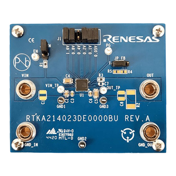
Page 7: Quick Start Guide
3. Populate the R4 and R5 feedback resistor divider for the required V 4. Connect the input supply to VIN and GND_IN. 5. Connect the load to OUT and GND_OUT. 6. Observe the output voltage. Board Design Figure 5. RTKA214023DE0000BU Evaluation Board R16UZ0020EU0100 Rev.1.00 Page 7 Sep 16, 2021... -
Page 8: Layout Guidelines
The trace for FB must be away from noisy planes and traces. The large 2.05mm x 2.05mm thermal pad under the 5mm x 5mm RAA214023 is connected to a large ground copper plane on the bottom layer for effective thermal dissipation.RTKA214023DE0000BU Evaluation Board Schematic Drawing Figure 6. -
Page 9: Bill Of Materials
RTKA214023DE0000BU Evaluation Board Manual Bill of Materials Reference Manufacturer Designator Description Part Number CAP-AEC-Q200, SMD, 0805, 10µF, 10V, 10%, X7R, Murata GCJ21BR71A106KE01L ROHS CAP, SMD, 1206, 22µF, 10V, 10%, X7R, ROHS Murata GRM31CR71A226KE15L CAP, SMD, 0603, DNP Generic Various C3, C6 CAP, SMD, 0603, 0.1µF, 16V, 10%, X7R, ROHS... -
Page 10: Typical Performance Curves
RTKA214023DE0000BU Evaluation Board Manual Figure 9. Bottom Layer Typical Performance Curves 100,000.0 10,000.0 IOUT = 10mA, 6.4μVRMS CSET = 100nF, 6.8μVRMS IOUT = 100mA, 6.3μVRMS CSET = 1μF, 6.5μVRMS 10,000.0 1,000.0 IOUT = 500mA, 6.2μVRMS CSET = 10μF, 6.4μVRMS 1,000.0 IOUT = 1A, 6.2μVRMS... -
Page 11: Ordering Information
RTKA214023DE0000BU Evaluation Board Manual Ordering Information Part Number Description RTKA214023DE0000BU RAA214023 evaluation board Revision History Rev. Date Description 1.00 Sep 16, 2021 Initial release R16UZ0020EU0100 Rev.1.00 Page 11 Sep 16, 2021... - Page 12 Renesas' products are provided only subject to Renesas' Terms and Conditions of Sale or other applicable terms agreed to in writing. No use of any Renesas resources expands or otherwise alters any applicable warranties or warranty disclaimers for these products.
Need help?
Do you have a question about the RTKA214023DE0000BU and is the answer not in the manual?
Questions and answers