Table of Contents
Advertisement
Quick Links
RTKA210030DR0000BU
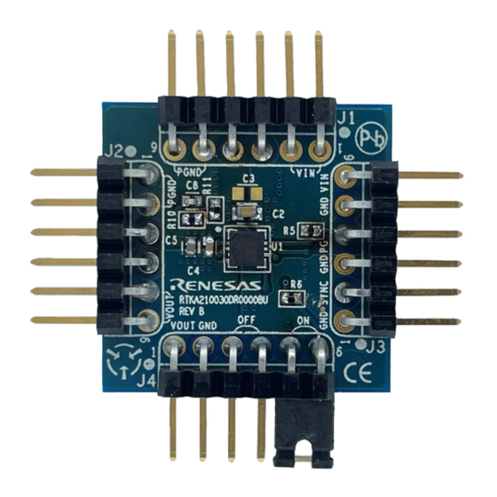
The RTKA210030DR0000BU demonstration board
(shown in
Figure 2
and
RTKA210030DR0000BU. Capable of delivering up to
3A of continuous current, the
compact, synchronous step-down, non-isolated
complete power supply that is optimized for
space-constrained applications. The
RTKA210030DR0000BU is based on a peak current
mode PWM control scheme that provides a fast
transient response and excellent loop stability. The
switching frequency is programmable from 500kHz to
4MHz with either the external resistor or
synchronization to an external clock through the
SYNC pin.
The RTKA210030DR0000BU demonstration board is
a 1×1 inch 4-layer FR4 board with 2oz. copper on
external layers and 1oz. copper on internal layers. It is
optimized to minimize the complete power module
solution size. Operating from a single 2.7V to 5.5V
input power rail, the RTKA210030DR0000BU
demonstration board offers adjustable output voltages
down to 0.6V, up to 95% efficiency, and better than
±1.5% accuracy over line, load, and temperature. A
dedicated enable pin and power-good flag allow for
easy system power rails sequencing.
By default, the board is set to a 1.8V output voltage
with a 2MHz switching frequency.
2.7V to 5.5V Input
22µF
100k
R16UZ0044EU0100 Rev.1.00
May 28, 2022
Figure
3) features the
RAA210030
is a
VIN
FS
EN
COMP
SYNC
PGND
Figure 1. Block Diagram
Demonstration Board Manual
Features
▪ Wide input voltage range from 2.7V to 5.5V
▪ Adjustable output voltage down to 0.6V with ±1.5%
accuracy over line, load, and temperature
▪ Up to 95% conversion efficiency
▪ 100% duty cycle
▪ Internal 1ms soft-start time
▪ Pre-bias output start-up
▪ External frequency synchronization up to 4MHz
▪ Dedicated enable pin and PGOOD flag
▪ UVLO, overcurrent, negative overcurrent,
overvoltage, and over-temperature protections
Specifications
The demonstration board is configured and optimized
for the following operating conditions:
▪ V
= 2.7V to 5.5V
IN
▪ V
= 1.8V
OUT
▪ I
OUT-MAX
▪ f
= 2MHz
SW
RAA210030
VOUT
FB
SGND
PGOOD
= 3A
1.8V 3A Output
22µFx2
100k
10pF
50k
Power-Good
© 2022 Renesas Electronics
Page 1
Advertisement
Table of Contents

Subscribe to Our Youtube Channel
Related Manuals for Renesas RTKA210030DR0000BU


Summary of Contents for Renesas RTKA210030DR0000BU
- Page 1 ▪ Up to 95% conversion efficiency complete power supply that is optimized for space-constrained applications. The ▪ 100% duty cycle RTKA210030DR0000BU is based on a peak current ▪ Internal 1ms soft-start time mode PWM control scheme that provides a fast ▪ Pre-bias output start-up transient response and excellent loop stability.
-
Page 2: Table Of Contents
RTKA210030DR0000BU Demonstration Board Manual Contents Functional Description ..............3 Recommended Testing Equipment . -
Page 3: Functional Description
RTKA210030DR0000BU Demonstration Board Manual Functional Description The RTKA210030DR0000BU provides the peripheral circuitry to demonstrate the feature set of the RAA210030. The demonstration board includes several connectors that simplify the validation of the module. The module is enabled and disabled by moving the jumper across the J4.3-J4.6 as shown in Figure 2. -
Page 4: Thermal Considerations And Current Derating
5. To enable external frequency synchronization, remove the pull-up resistor R of the SYNC pin and connect the external clock to J3.2 (SYNC). To ensure proper operation, Renesas recommends that the external SYNC frequency is within ±25% of the switching frequency set by R at the FS pin. -
Page 5: Layout Guidelines
Figure 3. RTKA210030DR0000BU Evaluation Board (Bottom) Layout Guidelines The RTKA210030DR0000BU demonstration board is a 1x1 inch four-layer FR-4 board with 2oz copper on external layers and 1oz copper on internal layers. The board can be used as a single 3A reference design. See... - Page 6 RTKA210030DR0000BU Demonstration Board Manual PGND SGND VOUT Figure 4. Layout Example - Top Layer PGND VOUT Figure 5. Layout Example - Bottom Layer RAA210610 SGND Pad Inner Layer PGND SGND Inner Layer RAA210610 PGND Pad Inner Layer Sl t i PCB Figure 6.
-
Page 7: Schematic Diagrams
RTKA210030DR0000BU Demonstration Board Manual Schematic Diagrams Figure 7. RTKA210030DR0000BU Schematic R16UZ0044EU0100 Rev.1.00 Page 7 May 28, 2022... -
Page 8: Bill Of Materials
RTKA210030DR0000BU Demonstration Board Manual Bill of Materials Reference Manufacturer Manufacture Part Number Designators IC-3A,5V,DC/DC STEP-DOWN PWR MODULE, Renesas RAA210030 10P, DFN, 3×3, ROHS CAP-POL, SMD, 47µF, 70mΩ, 20%,10V Panasonic 10TAB47M CAP, SMD, 0603, 22µF, 10V, 20%, X5R, ROHS Murata GRM188R61A226ME15D... - Page 9 RTKA210030DR0000BU Demonstration Board Manual Figure 10. Layer 2 Figure 11. Layer 3 Figure 12. Layer 4 Figure 13. Silkscreen Bottom R16UZ0044EU0100 Rev.1.00 Page 9 May 28, 2022...
-
Page 10: Typical Performance Graphs
RTKA210030DR0000BU Demonstration Board Manual Typical Performance Graphs The following data was acquired using the RTKA210030DR0000BU demonstration board at +25C ambient and free air 0LFM. Operating condition: V = 1.8V, f = 2MHz, unless otherwise noted. See the Table 1 for recommended configurations for different output voltages. - Page 11 RTKA210030DR0000BU Demonstration Board Manual Operating condition: V = 1.8V, f = 2MHz, unless otherwise noted. See the Table 1 for recommended configurations for different output voltages. (Cont.) 50mV/Div 50mV/Div 2A/Div 2A/Div 40µs/Div 40µs/Div Figure 21. Transient Response, V = 3.3V, V = 1.8V,...
- Page 12 RTKA210030DR0000BU Demonstration Board Manual Operating condition: V = 1.8V, f = 2MHz, unless otherwise noted. See the Table 1 for recommended configurations for different output voltages. (Cont.) 50mV/Div 50mV/Div 2A/Div 2A/Div 40µs/Div 40µs/Div Figure 26. Transient Response, V = 5V, V = 1.8V,...
-
Page 13: Ordering Information
RTKA210030DR0000BU Demonstration Board Manual Operating condition: V = 1.8V, f = 2MHz, unless otherwise noted. See the Table 1 for recommended configurations for different output voltages. (Cont.) 0LFM 200LFM 400LFM Temperature (°C) Figure 32. Derating Curve, V = 5V, V = 1.8V, C... - Page 14 Renesas' products are provided only subject to Renesas' Terms and Conditions of Sale or other applicable terms agreed to in writing. No use of any Renesas resources expands or otherwise alters any applicable warranties or warranty disclaimers for these products.
Need help?
Do you have a question about the RTKA210030DR0000BU and is the answer not in the manual?
Questions and answers