
Related Manuals for S&T Kontron VX3060


Summary of Contents for S&T Kontron VX3060
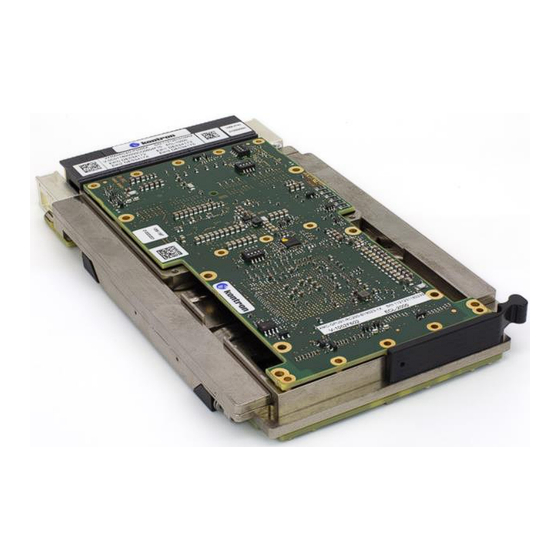
- Page 1 USER GUIDE VX3060 & VX3060-S2 3U VPX Computing Node D247914-V1.2 – Apr 2022 www.kontron.com // 2...
- Page 2 VX3060 & VX3060-S2 User Guide – D247914-V1.2 VX3060 & VX3060-S2 User Guide Disclaimer Kontron would like to point out that the information contained in this user guide may be subject to alteration, particularly as a result of the constant upgrading of Kontron products. This document does not entail any guarantee on the part of Kontron with respect to technical processes described in the user guide or any product characteristics set out in the user guide.
- Page 3 VX3060 & VX3060-S2 User Guide – D247914-V1.2 Revision History Publication Title: VX3060 User Guide Doc. ID: D247914 Revision Brief Description of Changes Date of Issue Initial issue Jan-2022 Latest updates added and tracked by change bars in the left document margin 28-Apr-2022 Section 1.3.2: Block diagram updated 29-Apr-2022...
- Page 4 VX3060 & VX3060-S2 User Guide – D247914-V1.2 Customer Support Please contact our support team at support.KFR@kontron.com Customer Service As a trusted technology innovator and global solutions provider, Kontron extends its embedded market strengths into a services portfolio allowing companies to break the barriers of traditional product lifecycles. Proven product expertise coupled with collaborative and highly-experienced support enables Kontron to provide exceptional peace of mind to build and maintain successful products.
- Page 5 VX3060 & VX3060-S2 User Guide – D247914-V1.2 Symbols The following symbols may be used in this user guide DANGER indicates a hazardous situation which, if not avoided, will result in death or serious injury. WARNING indicates a hazardous situation which, if not avoided, could result in death or serious injury.
- Page 6 VX3060 & VX3060-S2 User Guide – D247914-V1.2 For Your Safety Your new Kontron product was developed and tested carefully to provide all features necessary to ensure its compliance with electrical safety requirements. It was also designed for a long fault-free life. However, the life expectancy of your product can be drastically reduced by improper treatment during unpacking and installation.
- Page 7 VX3060 & VX3060-S2 User Guide – D247914-V1.2 General Instructions on Usage In order to maintain Kontron’s product warranty and CE compliance, this product must not be altered or modified in any way. Changes or modifications to the product, that are not explicitly approved by Kontron and described in this user guide or received from Kontron Support as a special handling instruction, will void your warranty and CE compliance.
-
Page 8: Table Of Contents
VX3060 & VX3060-S2 User Guide – D247914-V1.2 Table of Contents Introduction ..............................14 1.1. Manual Overview.............................. 15 1.1.1. Objective ..............................15 1.1.2. Audience ..............................15 1.1.3. Scope............................... 15 1.1.4. Structure ..............................15 1.1.5. Terminology, Definitions and Abbreviations ....................16 1.2. VPX Overview ..............................17 1.3. - Page 9 VX3060 & VX3060-S2 User Guide – D247914-V1.2 3.2. I2C Structure ..............................50 3.3. CPLD Features ..............................51 3.4. Serial Lines Additional Modes ..........................52 3.5. GPIOs and GDISCRETE1 ............................53 3.5.1. GPIOs ..............................53 3.5.2. GDISCRETE1 .............................. 53 3.6. Reset ................................53 3.7.
- Page 10 VX3060 & VX3060-S2 User Guide – D247914-V1.2 5.1.4. Output Powers Supplies Protection ......................80 5.2. VPX Input Power Rails Specification ........................81 5.3. Power Consumption Specification ........................83 5.3.1. VX3060 Thermal Power ..........................83 5.3.2. VX3060 Maximum Peak Current ........................83 5.4.
- Page 11 VX3060 & VX3060-S2 User Guide – D247914-V1.2 List of Figures Figure 1: VX3060 3U VPX view - Conduction cooled variant..................... 14 Figure 2: VX3060 3U VPX view – Air cooled variants ........................ 14 Figure 3: Block Diagrams ................................. 20 Figure 4: VX3060 SA variants - Front Panel I/O Interfaces......................25 Figure 5: VX3060 RC variants with XMC slot option - Front Panel I/O Interfaces................
- Page 12 VX3060 & VX3060-S2 User Guide – D247914-V1.2 List of Tables Table 1: Available SOSA variants Order Codes – Air cooled....................... 23 Table 2: Available SOSA variants Order Codes – Conduction cooled ..................23 Table 3: Available Order Codes – Air cooled ..........................24 Table 4: Available Order Codes –...
- Page 13 VX3060 & VX3060-S2 User Guide – D247914-V1.2 Table 51: VX3060 / Conduction cooled Typical Functional Points ..................... 90 Table 52: RTM Order Codes ..............................91 Table 53: PB-VX3-40G-602 Technical Specification ........................92 Table 54: PB-VX3-40G-602 Front Panel Connector Descriptions ....................93 Table 55: PB-VX3-40G-602 On-boards Connector Descriptions ....................
-
Page 14: 1/ Introduction
VX3060 & VX3060-S2 User Guide – D247914-V1.2 1/ Introduction The Kontron VX3060 is a 3U VPX computing blade for data and signal processing application focusing on application domains such as Military & Aerospace, Transportation and Energy/Industry. The Kontron VPX blade VX3060 is the ideal building block for intensive parallel computing workloads where a cluster of Kontron VX3060 can be used in switched OpenVPX environments. -
Page 15: Manual Overview
VX3060 & VX3060-S2 User Guide – D247914-V1.2 1.1. Manual Overview 1.1.1. Objective This guide provides general information, hardware instructions, operating instructions and functional description of the VX3060 board. The onboard programming, onboard firmware and other software (e.g. drivers and BSPs) are described in detail in separate guides (see section 1.7 "Related Publications"). -
Page 16: Terminology, Definitions And Abbreviations
VX3060 & VX3060-S2 User Guide – D247914-V1.2 1.1.5. Terminology, Definitions and Abbreviations > VX3060 and VX3060-S2 boards This User Guide describes the VX3060 and VX3060-S2 boards. The VX3060-S2 is fully compatible with system architectures developed in alignment with the SOSA™ technical standard. Another evolution of this architecture named just 'VX3060' has been designed for rear I/O compatibility with former Kontron SBC products. -
Page 17: Vpx Overview
VX3060 & VX3060-S2 User Guide – D247914-V1.2 Term or Acronym Definition Trusted Platform Module: An international standard for a secure cryptoprocessor based on a dedicated hardware device and integrating cryptographic keys. Promoted by consortium TCG (Trusted Computing Group). Turbo Boost A feature that opportunistically enables the processor to run a faster frequency. - Page 18 VX3060 & VX3060-S2 User Guide – D247914-V1.2 Features overview Processor 11th Gen Intel® Core™ Processor Family, enhanced AI, AVX-512, up to DDR4-3200 dual channel memory with IBECC, up to 32 Gbytes Numerous USB-C, USB2/3, PCIe/SATA options to front panel, VPX rear panel and XMC slot. Platform Controller Hub Integrated Intel®...
- Page 19 VX3060 & VX3060-S2 User Guide – D247914-V1.2 Software Kontron is one of the few compact PCI, VME and VPX vendors providing in-house support for most of the industry-proven real- time operating systems that are currently available. Thanks to its close relationship with the software editors, Kontron is able to locally produce and support BIOS, BSPs and drivers for the latest operating system revisions thereby taking advantage of the changes in technology which follow silicon evolution.
-
Page 20: Block Diagram
VX3060 & VX3060-S2 User Guide – D247914-V1.2 1.3.2. Block Diagrams Figure 3: Block Diagrams www.kontron.com // 20... - Page 21 VX3060 & VX3060-S2 User Guide – D247914-V1.2 L1 to L5 RESET EEPROM EEPROM ETH3 VX3060 Block Diagram ETH2 CPLD 1/2 DP x4 USB2/3 5 bicolor (Push- 256kbit 0xA0 256kbit 0xA2 Port COM1 LEDs button) MiniDP USB-C Board RJ45 EIA-232 RJ45 Connector Connector &Power...
-
Page 22: Ordering Information
VX3060 & VX3060-S2 User Guide – D247914-V1.2 1.3.3. Ordering Information Main Manufacturing Options Manufacturing Description Dependencies with other options Options Air cooled SA, WA, RA Conduction cooled RC3/RC4 Covers Environmental Class EVAL/ Lab-grade for customer assessments and Covers option not available on standard air-cooled products. developments Processor Type 11th Gen Intel®... -
Page 23: Table 1: Available Sosa Variants Order Codes - Air Cooled
VX3060 & VX3060-S2 User Guide – D247914-V1.2 Available Order Codes – SOSA variants (S2) Table 1: Available SOSA variants Order Codes – Air cooled Environmental Standard Order Description Class Codes 3U Single slot 5HP (1") VPX SBC EVAL/ Lab-grade VX3060-S2-SA4G-20EN00V1Q Air cooled @1.8GHz/15W, no conformal coating ®... -
Page 24: Table 3: Available Order Codes - Air Cooled
VX3060 & VX3060-S2 User Guide – D247914-V1.2 Available Order Codes – Non SOSA variants Table 3: Available Order Codes – Air cooled Environmental Standard Order Description Class Codes 3U Single slot 5HP (1") VPX SBC EVAL/ Lab-grade VX3060-SA4F-00PF01C1P Air-Cooled 'SA' @1.8GHz/15W Intel®... -
Page 25: I/O Interfaces
VX3060 & VX3060-S2 User Guide – D247914-V1.2 1.3.4. I/O Interfaces Front Interfaces Figure 4: VX3060 SA variants - Front Panel I/O Interfaces Table 5: Front I/O Interfaces FUNCTION DESCRIPTION SEE ALSO Reset push button Figure 4 LED indicators reporting the board CPU health status and activity Section 4.4 for LEDs Description USB0 USB type-C port –... - Page 26 VX3060 & VX3060-S2 User Guide – D247914-V1.2 Rear Interfaces Rear interfaces are compatible with the following: VX3060-S2 SOSA Slot profile compatible with SLT3-PAY-1F1F2U1TU1T1U1T-14.2.16 VX3060-S2 SOSA Module profile compatible with MOD3-PAY-1F1F2U1TU1T1U1T-16.2.15-2 VX3060 non SOSA Slot profiles compatible with SLT3-PAY-2F2U-14.2.3, SLT3-PAY-1F1F2U-14.2.4 and SLT3-PAY-1F1U-14.2.10. Refer to Section 4.3 for detailed VPX pin assignments and interfaces.
-
Page 27: Components Layout
VX3060 & VX3060-S2 User Guide – D247914-V1.2 1.3.5. Components Layout Figure 6: VX3060 Components Layout (Top view) DDR4 M2S1 M.2 slot TgL SoC 2242-M XMC Slot Figure 7: VX3060 Components Layout (Bottom view) M2S2 Bottom M.2 slot 2242-M www.kontron.com // 27... -
Page 28: M2 Module List
VX3060 & VX3060-S2 User Guide – D247914-V1.2 1.3.6. M2 Module List Table 6: Non-exhaustive M.2 module list, tested on VX3060 M.2 slots Upstream interface Tested Memory Module Type option selected on Capacity Manufacturer Part Number slot Technology the M.2 socket M2S1 SSD SATA, Type 2242 M SATA... -
Page 29: Environmental Specifications
VX3060 & VX3060-S2 User Guide – D247914-V1.2 1.4. Environmental Specifications Table 7: VX3060 – Standard and extended class - Environmental Specifications VX3060 Environmental class Standard Commercial Extended Temperature Plugin unit type 3U VPX Module Vita 46.0 October 2007 3U VPX Module Vita 46.0 October 2007 specification, specification, Type2, corrected by REDI VITA 48.1 Type2, corrected by REDI VITA 48.1 July 2010 (5HP) July 2010 (5HP) -
Page 30: Table 9: Vx3060 Lab-Grade Environmental Specifications For Prototypes Or Eval Variants
VX3060 & VX3060-S2 User Guide – D247914-V1.2 Table 9: VX3060 Lab-grade Environmental Specifications for Prototypes or EVAL Variants Lab-grade air-cooled version (1" single height passive module heat sink, forced air) Conformal Coating optional Inlet Airflow 3 m/s Cooling Method Convection or conduction Operating 10 °C to +30 °C Known product limitations... -
Page 31: Board Mass
VX3060 & VX3060-S2 User Guide – D247914-V1.2 1.5. Board Mass Table 10: VX3060 Mass VX3060 Mass VX3060-S2-RC34G-21EN00V10 ~ 550 g RC with XMC option & Without any module VX3060-SA4F-00PF01C1P ~ 650 g SA without any module 1.6. MTBF Data Table 11: VX3060 MTBF Data GB (Hours) MTBF 25 °C... -
Page 32: Related Publications
VX3060 & VX3060-S2 User Guide – D247914-V1.2 1.7. Related Publications The following publications contain information relating to this product: Table 12: Related Publications Standards Version Publication ANSI/VITA 46.0 ANSI/VITA 46.0-2007[R2013] VPX Baseline Standard ANSI/VITA 46.9 March 2018 XMC Rear I/O Fabric Signal Mapping on 3U and 6U VPX Modules ANSI/VITA 46.10 ANSI/VITA 46.10-2009... -
Page 33: 2/ Installation
VX3060 & VX3060-S2 User Guide – D247914-V1.2 2/ Installation The VX3060 has been designed for easy installation. However, the following standard precautions, installation procedures, and general information must be observed to ensure proper installation and to preclude damage to the board, other system components, or injury to personnel. -
Page 34: Board Identification
VX3060 & VX3060-S2 User Guide – D247914-V1.2 2.2. Board Identification The VX3060 boards are identified by labels fitted to the top side of the board. The E.C. Level format is "xxxxxLy" where The five digits "xxxxx" indicate the board E.C. Level (PCB revision included) ... -
Page 35: Board Configuration
VX3060 & VX3060-S2 User Guide – D247914-V1.2 2.3. Board Configuration 2.3.1. Microswitches Microswitch SW3 Figure 10: VX3060-S2 Board Configuration (Bottom view) Microswitch SW2 Microswitch SW1 www.kontron.com // 35... -
Page 36: Sw1 Microswitch Description
VX3060 & VX3060-S2 User Guide – D247914-V1.2 2.3.2. SW1 Microswitch Description Table 13: SW1 Microswitch Description Function Description OFF: Normal operating mode FACTORY_MODE ON : Enable special config for factory tests OFF: Normal operating mode VPD_WP ON : Force unprotection of devices in “VPD” domain OFF: Normal operating mode USER_WP ON : Force protection of devices in “USER”... -
Page 37: Package Contents
VX3060 & VX3060-S2 User Guide – D247914-V1.2 2.4. Package Contents The package contents vary with the VX3060 variant. Order Code: see section 1.3.3 “Order Code Table”: Board equipment differs depending on Order Code. Bolt accessories for mezzanine mounting (XMC and M2 modules). www.kontron.com // 37... -
Page 38: Initial Installation Procedures
VX3060 & VX3060-S2 User Guide – D247914-V1.2 2.5. Initial Installation Procedures The following procedures are applicable only for the initial installation of the VX3060 in a system. Procedures for standard removal operations are found in their respective chapters. To perform an initial installation of the VX3060 in a system, proceed as follows: Ensure that the safety requirements indicated in section 2.1 page 33 are observed. -
Page 39: Standard Removal Procedure
VX3060 & VX3060-S2 User Guide – D247914-V1.2 Running the board at high temperature without tightening the wedgelocks to the cold plate may result in permanent damage to the board. e. Ensure that the board is properly secured. The VX3060 is now ready for operation. Refer to appropriate VX3060 specific software, application, and system documentation. 2.6. -
Page 40: Xmc Module Insertion / Removal Instructions
VX3060 & VX3060-S2 User Guide – D247914-V1.2 2.7. XMC Module Insertion / Removal Instructions ESD sensitive Device! Precautions are listed in Section 2.1 Apply "Loctite 222e" threadlock on each screw during reassembly of the XMC Supported XMC type The default XMC connectors are VITA 61 XMC 2.0 compliant and support PCI-Express interface. XMC IOs connector (J16) is equipped by default. -
Page 41: Figure 14: Xmc And Xmc Cover Installation On A Rc Board Type
VX3060 & VX3060-S2 User Guide – D247914-V1.2 Figure 14: XMC and XMC cover Installation on a RC board type Article Description Torque 1064-4811 XMC cover 1058-7782 HEXALOBULAR SOCKET CHEESE HEAD SCREW ISO 14580-M2X5-A4-70 0.14 N.m 1058-7775 HEXALOBULAR SOCKET CHEESE HEAD SCREW ISO 14580-M2.5X6-A4-70 0.28 N.m 1058-7783 HEXALOBULAR SOCKET CHEESE HEAD SCREW ISO 14580-M2X6-A4-70... -
Page 42: Figure 15: Xmc Installation On A Sa Class Board Type
VX3060 & VX3060-S2 User Guide – D247914-V1.2 Figure 15: XMC Installation on a SA class board type Note : detailed description of 1058-7775 in Table of Figure 14. www.kontron.com // 42... -
Page 43: Figure 16: Xmc Module Removal
VX3060 & VX3060-S2 User Guide – D247914-V1.2 Unmating The XMC connectors can be unmated by pulling them straight apart or by “rocking” the connectors from side-to-side while pulling them apart. Figure 16: XMC Module Removal www.kontron.com // 43... -
Page 44: Module Insertion / Removal Instructions
VX3060 & VX3060-S2 User Guide – D247914-V1.2 2.8. M.2 Module Insertion / Removal Instructions Supported M.2 Module Type The M.2 sockets (M2S1 on top side and M2S2 on bottom side) are compliant with PCIe/SATA interfaces. The socket can host the following module types: 2242-XX-M with XX = S1, S2, S3, D1, D2, D3, D4, D5 ... -
Page 45: Figure 18: Top M.2 Module Insertion On A Rc Board Type (M2S1 Slot)
VX3060 & VX3060-S2 User Guide – D247914-V1.2 Figure 18: Top M.2 Module Insertion on a RC board type (M2S1 slot) Article DESCRIPTION Torque 1058-6013 WASHER ISO 7092-2-200HV-A4 1069-1981 M.2 SSD H5.2 spacer 1058-7785 HEXALOBULAR SOCKET CHEESE HEAD SCREW ISO 14580-M2X8-A4-70 0.14 N.m Figure 19: M.2 Module Insertion with threaded rod previously installed. -
Page 46: Figure 20: Adhesive Application Example To Lock M.2 Module On A Rugged Board
VX3060 & VX3060-S2 User Guide – D247914-V1.2 Figure 20: Adhesive application example to lock M.2 Module on a rugged board For harsh environment applications (RA or RC classes), Kontron recommends to apply an adhesive (such as Dowsil TM 3145 RTV-Clear or equivalent) at the junction between the module and the connector to improve the mechanical stability. -
Page 47: Figure 21: M.2 Module Removal Process
VX3060 & VX3060-S2 User Guide – D247914-V1.2 M.2 Module Removal Process Figure 21: M.2 Module Removal Process 1. Loosen the screw by hand and the module will be rotated automatically due to connector contact’s counterforce at the same time. 2. -
Page 48: Software Installation
VX3060 & VX3060-S2 User Guide – D247914-V1.2 2.9. Software Installation The installation of all onboard peripheral drivers is described in detail in the relevant Driver Kit files or Board Support Packages (BSP). The installation of an operating system is dependent of the OS software and is not addressed in this manual. Refer to appropriate OS software documentation for installation. -
Page 49: 3/ Additional Board Features
VX3060 & VX3060-S2 User Guide – D247914-V1.2 3/ Additional Board Features 3.1. RTC, Watchdog, Timers 3.1.1. Real-Time Clock (RTC) Two Real Time Clocks (RTC) are available on the VX3060: one is embedded in the PCH while the other is a standalone, high-precision, low-power component (RV-8803) accessed through the PCH SMBus. -
Page 50: Cpld Watchdog
VX3060 & VX3060-S2 User Guide – D247914-V1.2 3.1.2. CPLD Watchdog In addition to the standard watchdog timer included in the integrated PCH, the cPLD implements a hardware watchdog timer that can be used by the operating software to monitor the normal operation of the system. It is enabled by software, and once enabled must be restarted at regular intervals. -
Page 51: Cpld Features
VX3060 & VX3060-S2 User Guide – D247914-V1.2 PCH SMBus SLAVE DEVICES ON SOC SMBUS SMBUS BASE ADDRESS FEATURES INTERFACE (7bit/8bit) INA220 82H / 41H VS1 Current Monitoring RV-8803 64H / 32H External RTC Device XMC Slot A0H / 50H To XMC Mezzanine SMBus ... -
Page 52: Serial Lines Additional Modes
VX3060 & VX3060-S2 User Guide – D247914-V1.2 3.4. Serial Lines Additional Modes Serial ports location Serial lines are available both on front (see serial connector in section 4.1 Front Panel ) and rear (VPX P1 & P2 connectors in sections 4.3.2 to 4.3.6). -
Page 53: Gpios And Gdiscrete1
VX3060 & VX3060-S2 User Guide – D247914-V1.2 3.5. GPIOs and GDISCRETE1 3.5.1. GPIOs The VX3060 features 5 GPIOs managed by the CPLD. Refer to the Software Release Notes for further details on the GPIO driver. One GPIO is available on VPX P1 connector ... -
Page 54: Nvmro
VX3060 & VX3060-S2 User Guide – D247914-V1.2 3.7. NVMRO NVMRO is defined by the VITA 46.0 standard. Refer to this standard for a full description. All non-volatile devices are protected when NVMRO is asserted, except M.2 SSD and boot flash. M.2 SSD may be protected if the installed SSD module supports the Write Protect signal (WP#) on the pin 58 of the M. -
Page 55: Ipmi Option
VX3060 & VX3060-S2 User Guide – D247914-V1.2 3.8. IPMI Option The IPMI option is implemented by default on S2 variants and on demand on non-S2 variants. Contact the Kontron Technical support for more information. The VX3060-S2 embeds an IPMI controller so much so that the VX3060-S2 is considered as a FRU as per VITA 46.11. The IMPI controller is accessible through an IPMB bus or through a host Keyboard Controller Style (KCS) interface. -
Page 56: Kontron Security Solution
VX3060 & VX3060-S2 User Guide – D247914-V1.2 3.9. Kontron Security Solution The VX3060 answers digital security requirements with hardware enforced root of trust (secure elements). The VX3060 supports SEC-Line computer security offering: APPROTECT: Application integrity, confidentiality, only authorized copies ... -
Page 57: 4/ Physical I/O
VX3060 & VX3060-S2 User Guide – D247914-V1.2 4/ Physical I/O 4.1. Front panel Front panel connectors equipment according to the ordered product variant. 4.1.1. Serial Connector - COM1 This section describes the IEEE 1394 front connector carrying serial ports COM1 Table 17: Serial Connector Pin Assignment Figure 23: Serial Connector (IEEE 1394 Type) Signal... -
Page 58: Gigabit Ethernet Connector - Ports Eth2 & Eth3
VX3060 & VX3060-S2 User Guide – D247914-V1.2 Serial Cable Description Table 19: Standard Serial Cable Description Conn. A IEEE1394 Signal Conn. B SUBD9 Standard Kontron serial cable : Order code 1064-4995 (SERIAL CABLE IEEE1394/SUBD9 F) 4.1.2. Gigabit Ethernet Connector - Ports ETH2 & ETH3 This section describes the dual RJ45 front connector carrying 1000BASE-T Ethernet ports ETH0 &... -
Page 59: Standard Frontio Profile Option
VX3060 & VX3060-S2 User Guide – D247914-V1.2 Ethernet Cable Description The Ethernet cable should be at least CAT5e, with a maximum length of 100 meters. 4.1.3. Standard FrontIO profile Option 4.1.3.1. miniDP Connector This section describes the front panel minDP connector carrying the Display port interface. Table 22: miniDP connector –... -
Page 60: Front Panel Usbc Connector - Usb0
VX3060 & VX3060-S2 User Guide – D247914-V1.2 4.1.3.2. Front panel USBC Connector – USB0 This section describes the USB-C front panel connector Table 23: USB-C connector – front panel TX1+ TX1- VBUS VBUS RX1+ RX1- VBUS VBUS Description Description Ground return B12 GND Ground return SSTXp1 SuperSpeed differential pair #1, TX, positive... -
Page 61: Dual Usb-C Frontio Profile Option
VX3060 & VX3060-S2 User Guide – D247914-V1.2 4.1.4. Dual USB-C FrontIO profile Option Contact Kontron support for availability status www.kontron.com // 61... -
Page 62: Onboard Connectors
VX3060 & VX3060-S2 User Guide – D247914-V1.2 4.2. Onboard Connectors Figure 25: Onboard Connectors 1. J15 3. J16 2. M2S1 slot (M.2 2242-M) 4. Layer2 option www.kontron.com // 62... -
Page 63: Xmc J15 Connector Pin Assignments
VX3060 & VX3060-S2 User Guide – D247914-V1.2 4.2.1. XMC J15 Connector Pin Assignments The pin assignment of the J15 XMC PCI Express connector is compatible with VITA 61.0 pin definition. This interface is a PCI Express with 4 lanes coming from the CPU. Table 24: XMC J15 Connector Pin Assignments Row A Row B... - Page 64 VX3060 & VX3060-S2 User Guide – D247914-V1.2 MNEMONIC DIRECTION SIGNAL DEFINITION JTAG Data In as per VITA42.0. JTAG Data Out as per VITA42.0. JTAG Mode Select as per VITA42.0. TRST# JTAG Reset as per VITA42.0. PCIe TX/RX PCIe x4 differential transmit/receive pairs (as per VITA42.3) REFCLK+/-0 100MHz PCIe differential reference clock as per VITA42.3.
-
Page 65: Xmc J16 Connector Pin Assignment
VX3060 & VX3060-S2 User Guide – D247914-V1.2 4.2.2. XMC J16 Connector Pin Assignment XMC I/O signals are routed to the VPX P1 and P2 connectors according to X38s+X8d signal assignment as per VITA 46.9 section 4.6, except that in place of the X38s mapping, only the first four are available on J16 and VPX P2 (named X4s). Table 26: XMC J16 Connector Pin Assignment Row A Row B... -
Page 66: Top/Bottom M.2 Sockets - Pin Assignment
VX3060 & VX3060-S2 User Guide – D247914-V1.2 4.2.3. Top/Bottom M.2 sockets - Pin Assignment The M.2 top/bottom sockets are used to connect M.2 modules, key M for storage. PCIe or SATA mode can be selected using BIOS settings, and according to the product options. Refer to VX3060 Software release notes. -
Page 67: Layer2 Socket For Optional Mezzanine - Pin Assignment
VX3060 & VX3060-S2 User Guide – D247914-V1.2 MNEMONIC DIRECTIO SIGNAL DEFINITION 3.3V Logic ground. - PCI Express: LED_1# indicator as per PCI Express M.2 specification. LED1# / DAS_DSS# - SATA: Device Activity Signal /Disable Staggered Spinup as per SATA 3.2. DAS is not connected to a LED (which is the main purpose of this signal) and DSS is not used since the devices are SSD and not hard drives (no spinup). -
Page 68: Rear Connectors
VX3060 & VX3060-S2 User Guide – D247914-V1.2 4.3. Rear Connectors VPX Bus Interface The complete 3U VPX connectors configuration comprises three connectors named P0 to P2: 8-wafer 7-row connector. P1 - P2: 16-wafer 7-row differential connectors. Figure 26: VPX Connectors www.kontron.com // 68... -
Page 69: Vx3060-S2 - Vpx P0 Connector
VX3060 & VX3060-S2 User Guide – D247914-V1.2 4.3.1. VX3060-S2 - VPX P0 Connector Table 30: VX3060-S2 - VPX Connector P0 Wafer Assignment WAFER ROW G ROW F ROW E ROW D ROW C ROW B ROW A +12V +12V +12V +12V +12V +12V... -
Page 70: Vx3060-S2 - Vpx P1 Connector
VX3060 & VX3060-S2 User Guide – D247914-V1.2 4.3.2. VX3060-S2 - VPX P1 Connector Table 32: VX3060-S2 - VPX Connector P1 Wafer Assignment Gdiscrete 1 DP PCIe TX0- DP PCIe TX0+ DP PCIe RX0- DP PCIe RX0+ [DP PCIe TX1-] [DP PCIe TX1+] [DP PCIe RX1-] [DP PCIe RX1+] VBAT... -
Page 71: Vx3060-S2 - Vpx P2 Connector
VX3060 & VX3060-S2 User Guide – D247914-V1.2 4.3.3. VX3060-S2 - VPX P2 Connector Table 34: VX3060-S2 - VPX Connector P2 Wafer Assignment COM2 TXD- VID L1- VID L1+ VID L0- VID L0+ (COM2 TXD) VID L3- VID L3+ VID L2- VID L2+ COM2 TXD+ VID PWR... -
Page 72: Vx3060 - Vpx P0 Connector (Non S2 Variants)
VX3060 & VX3060-S2 User Guide – D247914-V1.2 4.3.4. VX3060 - VPX P0 Connector (non S2 variants) Table 36: VX3060 (non S2 variants) - VPX Connector P0 Wafer Assignment WAFER ROW G ROW F ROW E ROW D ROW C ROW B ROW A +12V +12V... -
Page 73: Vx3060 - Vpx P1 Connector (Non S2 Variants)
VX3060 & VX3060-S2 User Guide – D247914-V1.2 4.3.5. VX3060 - VPX P1 Connector (non S2 variants) Table 38: VX3060 (non S2 variants) - VPX Connector P1 Wafer Assignment Gdiscrete 1 DP PCIe TX0- DP PCIe TX0+ DP PCIe RX0- DP PCIe RX0+ [DP PCIe TX1-] [DP PCIe TX1+] [DP PCIe RX1-]... -
Page 74: Vx3060 - Vpx P2 Connector (Non S2 Variants)
VX3060 & VX3060-S2 User Guide – D247914-V1.2 4.3.6. VX3060 - VPX P2 Connector (non S2 variants) Table 40: VX3060 (non S2 variants) - VPX Connector P2 Wafer Assignment COM1 RTS/TXD- COM1 USB PWR USB PWR USB PWR TXD/TXD+ USB3 D0- USB3 D0+ USB2 D1- USB2 D1+... -
Page 75: Leds
VX3060 & VX3060-S2 User Guide – D247914-V1.2 4.4. LEDs 4.4.1. Status LEDs Default Setting There are five bicolor LEDs (Red/Green) on the front panel of the VX3060 3U VPX board. Figure 27: Front panel LEDs 4.4.2. LEDs Activity – Normal Mode When LED1 is red, the meaning of the other LEDs is changed. -
Page 76: Table 42: Leds Description - Normal Mode
VX3060 & VX3060-S2 User Guide – D247914-V1.2 Table 42: LEDs Description - Normal Mode LED1 Board fully off GREEN Board running. Blinking slow (@1Hz) when off/sleeping and no reset source is active. ORANGE Board reset asserted. Blinking slow (@1Hz) when off/sleeping and a reset source is active. Fatal error. -
Page 77: Power Sequencer/Error Codes (Leds)
VX3060 & VX3060-S2 User Guide – D247914-V1.2 4.4.3. Power Sequencer/Error codes (LEDs) When in "debug mode", the LEDs no more have their operational meaning, but LED1 is blinking green fast (@2Hz), and LED2, LED3, LED4, LED5 are displaying the current power state as follows : Table 43: LEDs Description –... -
Page 78: 5/ Power And Thermal Specifications
VX3060 & VX3060-S2 User Guide – D247914-V1.2 5/ Power and Thermal Specifications 5.1. Power Consideration The considerations presented in the ensuing sections must be taken into account by system integrators when specifying the VX3060 system environment. 5.1.1. Backplane Backplanes to be used with the VX3060 must be adequately specified and comply with VITA 65.0. The backplane must provide optimal power distribution for the VPX VS1, VS2, VS3 and 3V3 AUX power inputs. -
Page 79: Power Supplies Monitoring
VX3060 & VX3060-S2 User Guide – D247914-V1.2 Regulation The system power supplies should be monotonic as they ramp to their specified final values during power up conditions as per VITA 46.0, section 3.2.2. The system power supplies shall be unconditionally stable under line, load, unload and transient load conditions including capacitive loads. -
Page 80: Output Powers Supplies Protection
VX3060 & VX3060-S2 User Guide – D247914-V1.2 5.1.4. Output Powers Supplies Protection On the VX3060, all the output power supplies provided on connectors are protected by fuse or current-limiting devices as described in the following table. Table 44: Output Powers Supplies Protection Port Function Location... -
Page 81: Vpx Input Power Rails Specification
VX3060 & VX3060-S2 User Guide – D247914-V1.2 5.2. VPX Input Power Rails Specification The VX3060 board has been designed for optimal power input and distribution. Still it is necessary to observe certain criteria essential for application stability and reliability. Absolute Maximum Input Voltage The table below indicates the absolute maximum input voltage ratings that must not be exceeded. -
Page 82: Table 47: Input Powers Supplies Protection
VX3060 & VX3060-S2 User Guide – D247914-V1.2 Input Power Supply Protection The input power rails are protected on the VX3060 by fuse as described in the following table. To prevent safety hazards, the chassis power supply must not exceed the Voltage Rating and Interrupt Rating of the fuse. Table 47: Input Powers Supplies Protection VPX VS1 VPX 3.3 V AUX... -
Page 83: Power Consumption Specification
VX3060 & VX3060-S2 User Guide – D247914-V1.2 5.3. Power Consumption Specification 5.3.1. VX3060 Thermal Power The following data show total board consumption for different processor configuration and Thermal Design Power. These data help for thermal power dissipation analysis. Table 48: Thermal Power: board power based on current measurements Max VPX VS1 Measured Average VPX VS1... -
Page 84: Board Thermal Monitoring
VX3060 & VX3060-S2 User Guide – D247914-V1.2 5.4. Board Thermal Monitoring To ensure long-term reliability of the VX3060, onboard components must not operate beyond their specified maximum temperature. The most critical component on the VX3060 is the processor. Operating the VX3060 above the maximum operating limits will result in permanent damage to the board. - Page 85 VX3060 & VX3060-S2 User Guide – D247914-V1.2 NCT7802Y Key specifications: Voltage monitoring accuracy +-10 mV Temperature Sensor Accuracy On-chip Temperature Sensor Accuracy (25~70 °C) +- 2 °C typ. On-chip Temperature Sensor Resolution 1 °C Operating Temperature Range -40 °C ~ 85 °C www.kontron.com // 85...
-
Page 86: Soc Thermal Monitoring
VX3060 & VX3060-S2 User Guide – D247914-V1.2 5.5. SoC Thermal Monitoring To allow optimal operation and long-term reliability of the VX3060, the processor must remain within the maximum junction temperature specifications. The maximum operating temperature for the processor die (TJMAX) is 100°C. The TJMAX temperature is the temperature not to exceed, to avoid entering the throttling mode with reduced performance. -
Page 87: Thermal Performance
VX3060 & VX3060-S2 User Guide – D247914-V1.2 5.6. Thermal Performance Board Level Thermal Performance The CPU core maximum junction temperature (TJ MAX) is the maximum temperature allowed before entering into throttling mode. The maximum operating temperature for the processor die (TJMAX) is 100°C. This core temperature is accessible through the Linux sensors driver. - Page 88 VX3060 & VX3060-S2 User Guide – D247914-V1.2 Turbo Boost When the processor is operating below these limits and the user’s workload demands additional performance, the processor frequency will dynamically increase until the upper limit of frequency is reached. Intel Turbo Boost Technology has multiple algorithms operating in parallel to manage current, power, and temperature to maximize performance and energy efficiency.
-
Page 89: Vx3060 / Air Cooled - Thermal Performance
VX3060 & VX3060-S2 User Guide – D247914-V1.2 5.7. VX3060 / Air cooled - Thermal Performance Figures below illustrates the operational limits of the VX3060 air cooled variants. The junction temperature of processor is kept below the maximum allowed to avoid the processors entering the throttling mode. The measurements were made based on a 5HP slot (1 inch height) and using Power Thermal Utility (PTU) software from Intel to adjust processor workload. -
Page 90: Vx3060 / Conduction Cooled Cooled - Thermal Performance
VX3060 & VX3060-S2 User Guide – D247914-V1.2 5.8. VX3060 / Conduction cooled cooled - Thermal Performance Card Edge Temperature Measurement The card edge temperature is measured as follows: the middle point in the wedgelock channel on the heat frame (refer to the red arrow, applicable to the left and rear sides). -
Page 91: 6/ Rtm Characteristics
The Kontron PB-VX3-40G-602 is a 3U VPX Rear Transition Module compliant with the definition of the Rear Transition Module on VPX Standard –VITA 46.10. It provides rear I/O peripherals connectivity for Kontron VX3060-S2 Single Board Computers. Figure 30: PB-VX3-40G-602 3U VPX Overview 6.1.2. -
Page 92: Technical Specification
VX3060 & VX3060-S2 User Guide – D247914-V1.2 6.1.3. Technical Specification Table 53: PB-VX3-40G-602 Technical Specification TECHNICAL SPECIFICATIONS Power Specification Supply Voltage 5V VS3 VPX, 12V VS1 VPX Consumption < 1A USB Ports maximum current Mechanical Specification Front Panel size 1 slot (5HP) for PB-VX3-40G-602 Dimension (mm) 100 x 81.5 Weight (g) -
Page 93: Front Panel Interfaces
VX3060 & VX3060-S2 User Guide – D247914-V1.2 6.1.4. Front Panel Interfaces Figure 31: PB-VX3-40G- 602 Front Panel I/O Interfaces USB 2.0 10 GETH port 2 SFP+ Maintenance Ports USB 2.0 or GB ETH USB 3.0 port 1 1000BASE-T Table 54: PB-VX3-40G-602 Front Panel Connector Descriptions Front Panel Name Description Comment... -
Page 94: On-Boards Interfaces
VX3060 & VX3060-S2 User Guide – D247914-V1.2 6.1.5. On-boards Interfaces The PB-VX3-40G-602 implements on-boards connectors in order to provide access to additional I/O interfaces such as SATA, COM2 serial line, GPIOs and PCIe. Figure 32: PB-VX3-40G-602 On-board I/O Interfaces (top) 1. -
Page 95: Table 55: Pb-Vx3-40G-602 On-Boards Connector Descriptions
VX3060 & VX3060-S2 User Guide – D247914-V1.2 1. J0602 4. J0402 7. J1801 2. J0601 5. P1101 3. J0403 6. J0401 Table 55: PB-VX3-40G-602 On-boards Connector Descriptions Connector Name Description Comment XMC IO PIM2 connector Refer to section 6.3.2.4 for the pinout J0602 assignment. -
Page 96: Installation
VX3060 & VX3060-S2 User Guide – D247914-V1.2 6.2. Installation The PB-VX3-40G-602 has been designed for easy installation. However, the following standard precautions, installation procedures, and general information must be observed to ensure proper installation and to preclude damage to the board, other system components, or injury to personnel. -
Page 97: Microswitches
VX3060 & VX3060-S2 User Guide – D247914-V1.2 6.2.3. Microswitches Two microswitches are available on the PB-VX3-40G-602: SW0301 and SW0401 Figure 35: PB-VX3-40G-602 Microswitch Location SW0401 SW0301 www.kontron.com // 97... -
Page 98: Sw0301 Microswitch Description
VX3060 & VX3060-S2 User Guide – D247914-V1.2 6.2.4. SW0301 Microswitch Description Table 56: SW0301 Microswitch Description FUNCTION DESCRIPTION 1 – EEPROM WP off: The 10Gb Ethernet retimer EEPROM is write protected Default setting The EEPROM is not write protected 2 – Reserved Used for test and debug purpose only. -
Page 99: Initial Installation Procedure
VX3060 & VX3060-S2 User Guide – D247914-V1.2 6.2.7. Initial Installation Procedure The following procedures are applicable only for the initial installation of the PB-VX3-40G-602 in a system. Procedures for standard removal operations are found in their respective chapters. To perform an initial installation of the PB-VX3-40G-602 in a system proceed as follows: Ensure that the safety requirements indicated in section 6.2.1 are observed. -
Page 100: Standard Removal Procedure
VX3060 & VX3060-S2 User Guide – D247914-V1.2 6.2.8. Standard Removal Procedure ESD sensitive Device! Precautions are listed in Section 2.1 To remove the board from the chassis proceeds as follows: Ensure that the safety requirements indicated in section 6.2.1 are observed. Care must be taken when applying the procedures below to ensure that neither the PB-VX3-40G-602 nor system boards are physically damaged by the application of these procedures. -
Page 101: Physical I/O
VX3060 & VX3060-S2 User Guide – D247914-V1.2 6.3. Physical I/O 6.3.1. Front Panel 6.3.1.1. Maintenance Port Connector The PB-VX3-40G-602 provides one serial maintenance port, COM1 on front panel RJ12 connector. COM1 operate either in EIA-232 mode only (simplified RX/TX) or in 3.3V LVCMOS level signaling without hardware modification. Defaults setting are: ... -
Page 102: Usb 2.0 Connector
VX3060 & VX3060-S2 User Guide – D247914-V1.2 DB9 A Pin DB9 B Pin Signal RJ-12 Pin Connector Connector Connector TXD1 TXD0 RXD0 RXD1 DB9 A of cable KIT-2X-RJ12DB9 shall be used with PB-VX3-40G-602 to access to maintenance port (COM1) of VX3060-S2 board. 6.3.1.2. -
Page 103: Spf+ Connector
VX3060 & VX3060-S2 User Guide – D247914-V1.2 Table 61: USB 3.0 Connector Pin Assignment Figure 40: USB 3.0 Connector SIGNAL function VBUS Protected by 1.5A fuse USB_D- Differential USB- USB_D+ Differential USB+ Logic Ground Negative SuperSpeed receiver STDA_SSRX- differential pair Positive SuperSpeed receiver STDA_SSRX+ differential pair... -
Page 104: Mini Displayport Connector
VX3060 & VX3060-S2 User Guide – D247914-V1.2 Table 62: Gigabit Ethernet Connector Pin Assignment Figure 41: RJ45 Ethernet Connector 10BASE-T 100BASE-TX 1000BASE-T SIGNAL SIGNAL SIGNAL BI_DA+ BI_DA- BI_DB+ BI_DC+ BI_DC- BI_DB- BI_DD+ BI_DD- Shell Chassis Ground 6.3.1.6. Mini DIsplayPort Connector The PB-VX3-40G-602 provides a mini DP front connector offering DP graphics interface on front panel. -
Page 105: On-Board Connectors
VX3060 & VX3060-S2 User Guide – D247914-V1.2 6.3.2. On-Board Connectors In addition of front panel connectors, the PB-VX3-40G-602 implements on-boards connectors in order to provide access to extra I/O interfaces such as SATA, COM2 serial line, GPIOs and PCIe. Refer to section 6.1.5, “On-boards Interfaces” page 94 for connector location. 6.3.2.1. -
Page 106: Sata Connector
VX3060 & VX3060-S2 User Guide – D247914-V1.2 6.3.2.3. SATA connector The onboard SATA standard connector is used to connect a SATA HDD. The following table provides pinout information for the onboard SATA connector P1101: Table 66: SATA onboard P1101 Pinout Figure 44: SATA onboard Connector SIGNAL FUNCTION... -
Page 107: Figure 46: Pim Onboard Connector
VX3060 & VX3060-S2 User Guide – D247914-V1.2 SIGNAL SIGNAL +3V3_AUX XMCIO_DP5- XMCIO_DP5+ Table 68: XMCIO PIM1 Connector Signal Description MNEMONIC DESCRIPTION XMCIO_DP5-10 Differential pairs XMC I/O 5 to 10 and 15 to 19 as per to VITA 46.9 P1w9-X12d XMCIO_DP15-19 +5 Volts DC power (VS3 VPX supply). -
Page 108: I2C Connector
VX3060 & VX3060-S2 User Guide – D247914-V1.2 SIGNAL SIGNAL XMCIO_SE1 XMCIO_SE2 XMCIO_DP2- XMCIO_DP1- XMCIO_DP2+ XMCIO_DP1+ XMCIO_DP4- XMCIO_DP3- XMCIO_DP4+ XMCIO_DP3+ XMCIO_DP12- XMCIO_DP11- XMCIO_DP12+ XMCIO_DP11+ XMCIO_DP14- XMCIO_DP13- XMCIO_DP14+ XMCIO_DP13+ * signal active when low Table 70: XMCIO PIM2 Signal Description MNEMONIC DESCRIPTION XMCIO_DP20 Differential pairs XMC I/O 20 as per to VITA 46.9 P1w9-X12d XMCIO_DP1-8... -
Page 109: Pcie Slot
VX3060 & VX3060-S2 User Guide – D247914-V1.2 6.3.2.6. M.2 PCIe Slot The M.2 bottom socket (J1801 connector) is used to connect a M.2 module, key M for SSD storage. PCIe 4x Gen3 is the default interface of SSD storage module. The M.2 socket supports only 2242 form factor. -
Page 110: Rear I/O Connectors
VX3060 & VX3060-S2 User Guide – D247914-V1.2 Table 73: M.2 Module Socket Signal Description MNEMONIC DIRECTIO SIGNAL DEFINITION +3.3V power supply. 3.3V Logic ground. PCI Express: Receive differential pair as per PCI Express M.2 & PCI Express 3.0 PERn+/- specifications. PCI Express: PCI Express PERST# as per PCI Express M.2 specification, handled by CPLD PERST# (SYSRESET). -
Page 111: Table 74: Rear I/O Vpx Connector Rp0 Wafer Assignment
VX3060 & VX3060-S2 User Guide – D247914-V1.2 RP0 Wafer Assignment Table 74: Rear I/O VPX Connector RP0 Wafer Assignment Legend for Table 74: IPMB_B/A IPMB I2C bus GPIO7 GPIO7 USB1 USB1 power PCIe0 Lx-Tx/Rx x4 PCI-Express WAFER ROW G ROW F ROW E ROW D... -
Page 112: Table 76: Rear I/O Vpx Connector Rp1 Wafer Assignment
VX3060 & VX3060-S2 User Guide – D247914-V1.2 RP1 Wafer Assignment Table 76: Rear I/O VPX Connector RP1 Wafer Assignment Legend for Table 76: SATA SATA link 3 from PCH GPIOx / Maskable Reset General Purpose I/O x and maskable reset ETH1 TX/RX 10GBASEKR link 1 from integrated 10 GbE ETH2 DA/DB/DC/DD... -
Page 113: Table 78: Rear I/O Vpx Connector Rp2 Wafer Assignment
VX3060 & VX3060-S2 User Guide – D247914-V1.2 MNEMONIC SIGNAL DEFINITION Serial ATA. Transmit +/- SATA TX+/- Differential Data transmit and receive of USBSS link USBSS TX+/- RX+/- Differential Data pair of USB x USBx D+/- Not connected Ground RP2 Wafer Assignment Table 78: Rear I/O VPX Connector RP2 Wafer Assignment ... - Page 114 VX3060 & VX3060-S2 User Guide – D247914-V1.2 About Kontron – An S&R Company Kontron is a global leader in embedded computing technology (ECT). As a part of technology group S&T, Kontron offers a combined portfolio of secure hardware, middleware and services for Internet of Things (IoT) and Industry 4.0 applications.
Need help?
Do you have a question about the Kontron VX3060 and is the answer not in the manual?
Questions and answers