Sign In
Upload
Manuals
Brands
S&T Manuals
Computer Hardware
Kontron VX3060
S&T Kontron VX3060 Manuals
Manuals and User Guides for S&T Kontron VX3060. We have
1
S&T Kontron VX3060 manual available for free PDF download: User Manual
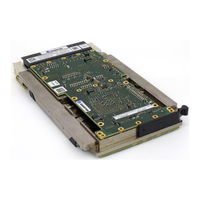
S&T Kontron VX3060 User Manual (114 pages)
3U VPX Computing Node
Brand:
S&T
| Category:
Computer Hardware
| Size: 5.7 MB
Table of Contents
Table of Contents
8
1/ Introduction
14
Figure 1: VX3060 3U VPX View - Conduction Cooled Variant
14
Figure 2: VX3060 3U VPX View - Air Cooled Variants
14
Manual Overview
15
Objective
15
Audience
15
Scope
15
Structure
15
Terminology, Definitions and Abbreviations
16
VPX Overview
17
Board Overview
17
Main Features
17
Block Diagram
20
Figure 3: Block Diagrams
20
Ordering Information
22
Table 1: Available SOSA Variants Order Codes - Air Cooled
23
Table 2: Available SOSA Variants Order Codes - Conduction Cooled
23
Table 3: Available Order Codes - Air Cooled
24
Table 4: Available Order Codes - Conduction Cooled
24
I/O Interfaces
25
Figure 4: VX3060 SA Variants - Front Panel I/O Interfaces
25
Figure 5: VX3060 RC Variants with XMC Slot Option - Front Panel I/O Interfaces
25
Table 5: Front I/O Interfaces
25
Components Layout
27
Figure 6: VX3060 Components Layout (Top View)
27
Figure 7: VX3060 Components Layout (Bottom View)
27
M2 Module List
28
Table 6: Non-Exhaustive M.2 Module List, Tested on VX3060 M.2 Slots
28
Environmental Specifications
29
Table 7: VX3060 - Standard and Extended Class - Environmental Specifications
29
Table 8: VX3060 - Rugged Class - Environmental Specifications
29
Table 9: VX3060 Lab-Grade Environmental Specifications for Prototypes or EVAL Variants
30
Board Mass
31
MTBF Data
31
Table 10: VX3060 Mass
31
Table 11: VX3060 MTBF Data
31
Related Publications
32
Table 12: Related Publications
32
2/ Installation
33
Safety Requirements
33
Board Identification
34
Figure 8: VX3060 Identification (Top Side)
34
Figure 9: VX3060 (Bottom Side, Without 2LM Option)
34
Board Configuration
35
Microswitches
35
Figure 10: VX3060-S2 Board Configuration (Bottom View)
35
SW1 Microswitch Description
36
SW2 Microswitch Description
36
SW3 Microswitch Description
36
Table 13: SW1 Microswitch Description
36
Table 14: SW2 Microswitch Description
36
Table 15: SW3 Microswitch Description
36
Package Contents
37
Initial Installation Procedures
38
Figure 11: VX3060 SA Board Insertion - Front Panel Retaining Screws Location
38
Figure 12: VX3060 RC Board Insertion - Wedgelock Screw Location
38
Standard Removal Procedure
39
XMC Module Insertion / Removal Instructions
40
Figure 13: XMC Module Insertion
40
Figure 14: XMC and XMC Cover Installation on a RC Board Type
41
Figure 15: XMC Installation on a SA Class Board Type
42
Figure 16: XMC Module Removal
43
Module Insertion / Removal Instructions
44
Figure 17: M.2 Module Insertion
44
Figure 18: Top M.2 Module Insertion on a RC Board Type (M2S1 Slot)
45
Figure 19: M.2 Module Insertion with Threaded Rod Previously Installed
45
Figure 20: Adhesive Application Example to Lock M.2 Module on a Rugged Board
46
Figure 21: M.2 Module Removal Process
47
Software Installation
48
3/ Additional Board Features
49
RTC, Watchdog, Timers
49
Real-Time Clock (RTC)
49
CPLD Watchdog
50
I2C Structure
50
Figure 22: I2C Diagram for Information
50
CPLD Features
51
Serial Lines Additional Modes
52
Gpios and GDISCRETE1
53
Gpios
53
Gdiscrete1
53
Reset
53
Table 16: Reset Management Table
53
Nvmro
54
IPMI Option
55
Kontron Security Solution
56
Approtect
56
Trusted Platform Module (TPM 2.0)
56
4/ Physical I/O
57
Front Panel
57
Serial Connector - COM1
57
Figure 23: Serial Connector (IEEE 1394 Type)
57
Table 17: Serial Connector Pin Assignment
57
Table 18: Serial Connector Signals Definition
57
Gigabit Ethernet Connector - Ports ETH2 & ETH3
58
Figure 24: RJ45 Tab-Down Ethernet Connector
58
Table 19: Standard Serial Cable Description
58
Table 20: Gigabit Ethernet Connector Pin Assignment
58
Table 21: Gigabit Ethernet Connector Signals Definition
58
Standard Frontio Profile Option
59
Minidp Connector
59
Table 22: Minidp Connector - Front Panel
59
Front Panel USBC Connector - USB0
60
Table 23: USB-C Connector - Front Panel
60
Dual USB-C Frontio Profile Option
61
Onboard Connectors
62
Figure 25: Onboard Connectors
62
XMC J15 Connector Pin Assignments
63
Table 24: XMC J15 Connector Pin Assignments
63
Table 25: XMC J15 Connector Signals Definition
63
XMC J16 Connector Pin Assignment
65
Table 26: XMC J16 Connector Pin Assignment
65
Table 27: XMC J16 Connector Signals Definition
65
Top/Bottom M.2 Sockets - Pin Assignment
66
Table 28: M.2 Socket Connector Pin Assignment
66
Table 29: M.2 Module Socket Signal Description
66
Layer2 Socket for Optional Mezzanine - Pin Assignment
67
Rear Connectors
68
Figure 26: VPX Connectors
68
VX3060-S2 - VPX P0 Connector
69
Table 30: VX3060-S2 - VPX Connector P0 Wafer Assignment
69
Table 31: VX3060-S2 - VPX Connector P0 Signal Definition
69
VX3060-S2 - VPX P1 Connector
70
Table 32: VX3060-S2 - VPX Connector P1 Wafer Assignment
70
Table 33: VX3060-S2 - VPX Connector P1 Signal Definition
70
VX3060-S2 - VPX P2 Connector
71
Table 34: VX3060-S2 - VPX Connector P2 Wafer Assignment
71
Table 35: VX3060-S2 - VPX Connector P2 Signal Definition
71
VX3060 - VPX P0 Connector (Non S2 Variants)
72
Table 36: VX3060 (Non S2 Variants) - VPX Connector P0 Wafer Assignment
72
Table 37: VX3060 (Non S2 Variants) - VPX Connector P0 Signal Definition
72
VX3060 - VPX P1 Connector (Non S2 Variants)
73
Table 38: VX3060 (Non S2 Variants) - VPX Connector P1 Wafer Assignment
73
Table 39: VX3060 (Non S2 Variants) - VPX Connector P1 Signal Definition
73
VX3060 - VPX P2 Connector (Non S2 Variants)
74
Table 40: VX3060 (Non S2 Variants) - VPX Connector P2 Wafer Assignment
74
Table 41: VX3060-S2 - VPX Connector P2 Signal Definition
74
Leds
75
Status Leds Default Setting
75
Leds Activity - Normal Mode
75
Figure 27: Front Panel Leds
75
Table 42: Leds Description - Normal Mode
76
Power Sequencer/Error Codes (Leds)
77
Table 43: Leds Description - Debug Mode / Error Codes
77
5/ Power and Thermal Specifications
78
Power Consideration
78
Backplane
78
Power Supply Units
78
Power Supplies Monitoring
79
Output Powers Supplies Protection
80
Table 44: Output Powers Supplies Protection
80
VPX Input Power Rails Specification
81
Table 45: Absolute Maximum Input Voltage
81
Table 46: Recommended Operating Input Voltage
81
Table 47: Input Powers Supplies Protection
82
Power Consumption Specification
83
VX3060 Thermal Power
83
VX3060 Maximum Peak Current
83
Table 48: Thermal Power: Board Power Based on Current Measurements
83
Table 49: Maximum VS1 Current
83
Board Thermal Monitoring
84
Figure 28: Temperature Sensor Location
84
Soc Thermal Monitoring
86
Thermal Performance
87
VX3060 / Air Cooled - Thermal Performance
89
Figure 29: VX3060 / Air Cooled Thermal Performance Curves
89
Table 50: VX3060 / Air Cooled Typical Functional Points
89
VX3060 / Conduction Cooled Cooled - Thermal Performance
90
Table 51: VX3060 / Conduction Cooled Typical Functional Points
90
6/ RTM Characteristics
91
Introduction
91
Overview
91
Ordering Information
91
Figure 30: PB-VX3-40G-602 3U VPX Overview
91
Table 52: RTM Order Codes
91
Technical Specification
92
Table 53: PB-VX3-40G-602 Technical Specification
92
Front Panel Interfaces
93
Figure 31: PB-VX3-40G- 602 Front Panel I/O Interfaces
93
Table 54: PB-VX3-40G-602 Front Panel Connector Descriptions
93
On-Boards Interfaces
94
Figure 32: PB-VX3-40G-602 On-Board I/O Interfaces (Top)
94
Figure 33: PB-VX3-40G-602 On-Board I/O Interfaces (Bottom)
94
Table 55: PB-VX3-40G-602 On-Boards Connector Descriptions
95
Installation
96
Safety Requirement
96
Identification
96
Figure 34: PB-VX3-40G-602 Identification
96
Microswitches
97
Figure 35: PB-VX3-40G-602 Microswitch Location
97
SW0301 Microswitch Description
98
SW0401 Microswitch Description
98
RTM Connectors Identification
98
Figure 36: Connectors Identification for PB-VX3-40G-602
98
Table 56: SW0301 Microswitch Description
98
Initial Installation Procedure
99
Standard Removal Procedure
100
Physical I/O
101
Front Panel
101
Maintenance Port Connector
101
Figure 37: Serial Connector
101
Figure 38: Serial Cable
101
Table 57: Serial Connector Pin Assignment
101
Table 58: Serial Connector Signal Description
101
Table 59: Serial Cable Pin Assignment
101
USB 2.0 Connector
102
USB 3.0 Connector
102
Figure 39: USB 2.0 Connector
102
Table 60: USB 2.0 Connector Pin Assignment
102
SPF+ Connector
103
Gigabit Ethernet Connector
103
Figure 40: USB 3.0 Connector
103
Table 61: USB 3.0 Connector Pin Assignment
103
Mini Displayport Connector
104
Figure 41: RJ45 Ethernet Connector
104
Table 62: Gigabit Ethernet Connector Pin Assignment
104
On-Board Connectors
105
COM2 Serial Line
105
GPIO Connector
105
Figure 42: HE10 J0401 Connector
105
Figure 43: HE10 J0402 Connector
105
Table 63: HE10 J0401 Pin Assignment
105
Table 64: Serial Connector Signal Description
105
Table 65: HE10 J0402 Pin Assignment
105
SATA Connector
106
XMC IO PIM Connectors
106
Figure 44: SATA Onboard Connector
106
Figure 45: PIM Onboard Connector
106
Table 66: SATA Onboard P1101 Pinout
106
Table 67: PIM1 Onboard J0601 Pinout
106
Figure 46: PIM Onboard Connector
107
Table 68: XMCIO PIM1 Connector Signal Description
107
Table 69: PIM2 Onboard J0602 Pinout
107
I2C Connector
108
Figure 47: I2C Onboard Connector
108
Table 70: XMCIO PIM2 Signal Description
108
Table 71: I2C Onboard J0403 Pinout
108
Pcie Slot
109
Table 72: J2801 M.2 Socket Pin Assignment
109
Rear I/O Connectors
110
Figure 48: Rear I/O VPX Connectors
110
Table 73: M.2 Module Socket Signal Description
110
Table 74: Rear I/O VPX Connector RP0 Wafer Assignment
111
Table 75: Rear I/O VPX Connector RP0 Signal Definition
111
Table 76: Rear I/O VPX Connector RP1 Wafer Assignment
112
Table 77: Rear I/O VPX Connector RP1 Signal Definition
112
Table 78: Rear I/O VPX Connector RP2 Wafer Assignment
113
Table 79: Rear I/O VPX Connector RP2 Signal Definition
113
Advertisement
Advertisement
Related Products
S&T Kontron VX3060-S2
S&T Kontron CP3005 Series
S&T Kontron CP3005-SA
S&T Kontron CP3005-V
S&T Kontron SMARC-sXEL
S&T Kontron SL iMX8MM
S&T kontron COMe-bV26
S&T kontron KBox E-420-R1K/V1K
S&T kontron COMe-cEL6
S&T Kontron COMe-cTL6
S&T Categories
Computer Hardware
Switch
Desktop
Motherboard
GPS
More S&T Manuals
Login
Sign In
OR
Sign in with Facebook
Sign in with Google
Upload manual
Upload from disk
Upload from URL