Table of Contents
Advertisement
Quick Links
UM2683
User manual
Inverse buck 35W with LED current controlled by HVLED002 with Analog/PWM
dimming regulation
Introduction
This document describes the EVAL-IBD002-35W demonstration board behavior, designed to manage a dimmable 35 W LED
load with a single inverse buck stage.
The HVLED002 controller manages the inverse buck circuit mainly composed by D1, L1 and Q1 components. This circuit
provides around 700 mA as maximum LED load current. The board operates in peak current mode with FOT (Fixed Off Time)
and it has been designed to operate with wide input (48 V - 60 V) and wide output (24 V - 48 V) voltages. The on-time changes
according to the operating condition to keep output current regulated and the switching frequency is consequently adapted.
In steady-state condition the pin COMP works at its maximum value because the FB signal is zero, providing the maximum
average current.. In this condition, decreasing VDimm input below 10 V, the Analog dimming circuit injects an ever higher offset
signal on HVLED002 current sense, so decreasing the output average current. When VDimm input voltage decreases under 2
V, the PWM Dimming circuit starts to generate a PWM output voltage with 5 V - 0 V amplitude. When PWM state is 0 V the FB
signal is zero providing the maximum average current and when the PWM state is 5 V the pin FB is pulled up to VREF and the
switching activity of HVLED002 is stopped providing zero output current. In this way, when the Vdimm is under 2 V, the output
average current increases/decreases depending on the PWM state condition. . Decreasing VDimm voltage level, the PWM high
level percentage increases, further decreasing the output average current too. So, the external 0 -10 V dimming signal is
dedicated to managing a dimmed output LED current between 1%-100% of its maximum value with both Analog control
100%÷10% (10 V÷2 V) and PWM control 10%÷1% (2 V÷0 V).
An external 15 Vdc of auxiliary voltage is needed to power up the HVLED002 controller while the D6, Q3 and U2 components
regulate a precise 12 V to the Vcc of HVLED002 and manage a constant pull-up voltage used for both dimming circuits.
The short-circuit protection is guaranteed by Zener diode D10 which detects a sudden fast slope rise of LED load Cathode
Voltage activating Q6 MOSFET and bringing the pin FB high and stopping the switching activity. On the PCB there are also
available (not mounted) the Discharge and OVP circuit positions, usable and useful with a primary stage connection (converter):
the first needed to discharge the C2 output capacitance after power turn-off and the second to stop the primary activity when an
Overvoltage occurs on the Output LED load.
UM2683 - Rev 1 - August 2020
www.st.com
For further information contact your local STMicroelectronics sales office.
Advertisement
Table of Contents

Related Manuals for ST EVAL-IBD002-35W


Summary of Contents for ST EVAL-IBD002-35W
- Page 1 Introduction This document describes the EVAL-IBD002-35W demonstration board behavior, designed to manage a dimmable 35 W LED load with a single inverse buck stage. The HVLED002 controller manages the inverse buck circuit mainly composed by D1, L1 and Q1 components. This circuit provides around 700 mA as maximum LED load current.
-
Page 2: Eval-Ibd002-35W Schematic Diagrams
UM2683 EVAL-IBD002-35W schematic diagrams EVAL-IBD002-35W schematic diagrams Figure 1. EVAL-IBD002-35W circuit schematic Vbus=48Vdc-60Vdc TP 1 TP 8 Vaux=15Vdc Vbus Vbus 12Vcc P WM Vaux TP 7 10uF 200k Vcc_unre g 100V 220k TS 321 S TP S 2H100AF 4.7uF VREF... -
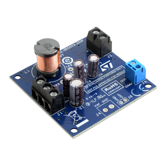
Page 3: Eval-Ibd002-35W Demonstration Board Layout
UM2683 EVAL-IBD002-35W demonstration board layout EVAL-IBD002-35W demonstration board layout Figure 2. EVAL-IBD002-35W component side UM2683 - Rev 1 page 3/24... -
Page 4: Figure 3. Eval-Ibd002-35W Solder Side
UM2683 EVAL-IBD002-35W demonstration board layout Figure 3. EVAL-IBD002-35W solder side UM2683 - Rev 1 page 4/24... -
Page 5: Eval-Ibd002-35W Demonstration Board Overview
Load Over 20% (analog dimming): > 95% Output ripple current max. <80mA@worst case 50Vindc-48Voutdc Short-circuit protection RoHS compliant Table 2 shows a Legend of all connector and Test Point available on the EVAL-IBD002-35W demonstration board Table 2. EVAL-IBD002-35W Connectors and Test Point description Reference Type Specs... -
Page 6: Eval-Ibd002-35W Measurement
Vdc and 50 Vdc. In both cases the Efficiency is 97% in Full Load conditions of 35 W (48 Vout-16LED) and higher than the 95% for Load over the 20% of its maximum Load. Figure 4. EVAL-IBD002-35W Efficiency vs. dimming@60Vindc Figure 5. EVAL-IBD002-35W Efficiency vs. dimming@48/50Vindc... -
Page 7: Eval-Ibd002-35W Set-Up
Auxiliary Voltage Dimming Here below a brief guide list to switch on the EVAL-IBD002-35W demonstration board: • Set the voltage of the Power Supply n.1 to 15 Vdc and from OFF conditions connect it to J1 with (+) to Vaux and (-) to GND;... -
Page 8: Eval-Ibd002-35W Waveforms
60 Vindc and Full Load (16LED) has been settled. As can be seen, no LED Iout and Vout overshoot have been highlighted during startup and that a 60mA output ripple current is managed during steady-state operations. Figure 7. EVAL-IBD002-35W startup 60Vindc Figure 8. EVAL-IBD002-35W steady-state 60Vindc... -
Page 9: Figure 11. Eval-Ibd002-35W Main Waveforms 60Vindc (16Led)
(ILED is around 155 mA) while in Figure14 with 1 V of dimming input voltage as highlighted, a PWM dimming with a hiccup current (ILED average is around 35 mA). Figure 13. EVAL-IBD002-35W VDIMM = 3 V 60Vindc Figure 14. EVAL-IBD002-35W VDIMM = 1 V 60Vindc... -
Page 10: Figure 15. Eval-Ibd002-35W Analog And Pwm Dimming Schematic
PWM output voltage with 5 V - 0 V amplitude, the FB pin is pulled up to VREF and the switching activity of HVLED002 is stopped as much as FB=VREF, further decreasing the output average current. Figure 15. EVAL-IBD002-35W Analog and PWM dimming schematic Dimming circuitry 12Vcc... -
Page 11: Figure 18. Eval-Ibd002-35W Vdimm = 1 V
UM2683 EVAL-IBD002-35W waveforms Figure 18. EVAL-IBD002-35W VDIMM = 1 V Figure 19. EVAL-IBD002-35W ILed average = 1% Ch.1: VGS (TP3) - Ch.2: VDimming (J6) Ch.1: VGS (TP3) - Ch.2: VDimming (J6) CCh.3: PWM dim/FB(TP8) - Ch.4: LED Output Current Ch.3: PWM dim/FB(TP8) - Ch.4: LED Output Current... -
Page 12: Figure 22. Eval-Ibd002-35W Vdimm = 0.5 V
UM2683 EVAL-IBD002-35W waveforms Figure 22. EVAL-IBD002-35W VDIMM = 0.5 V Figure 23. EVAL-IBD002-35W VDIMM = 0 V Ch.1: VGS (TP3) - Ch.2: VDimming (J6) Ch.1: VGS (TP3) - Ch.2: VDimming (J6) Ch.3: PWM dim/FB(TP8) - Ch.4: LED Output Current Ch.3: PWM dim/FB(TP8) - Ch.4: LED Output Current Figure 24 shows the ILed trend vs. -
Page 13: Figure 25. Dimming 1%÷20% Vs. Iled Output Current (Pwm Dimming Area)
UM2683 EVAL-IBD002-35W waveforms Figure 25 shows the PWM Dimming area detail of several settings (Vin and Vout) to show the linear current shape. Figure 25. Dimming 1%÷20% vs. ILed Output Current (PWM Dimming area) UM2683 - Rev 1 page 13/24... -
Page 14: Eval-Ibd002-35W Short-Circuit Protection
UM2683 EVAL-IBD002-35W short-circuit protection EVAL-IBD002-35W short-circuit protection Figure 26. EVAL-IBD002-35W output short-circuit Figure 27. EVAL-IBD002-35W output short-circuit 60Vindc (16LED) removal 60Vindc (16LED) Ch.1: VAnode (TP1) - Ch.2: VKathode (TP2) Ch.1: VAnode (TP1) - Ch.2: VKathode (TP2) Ch.3: VGS Q6 - Ch.4: LED Current + Ishort Ch.3: VGS Q6 - Ch.4: LED Current + Ishort... -
Page 15: Eval-Ibd002-35W Thermography
UM2683 EVAL-IBD002-35W thermography EVAL-IBD002-35W thermography Figure 30. EVAL-IBD002-35W 60 Vindc (16LED) - Figure 31. EVAL-IBD002-35W 60 Vindc (16LED) - Top View Bottom View A: L1 (pcb) Hottest Front area A: U1 - B: Q1 - C: R9 Figure 32. EVAL-IBD002-35W Short - Top View Figure 33. -
Page 16: Eval-Ibd002-35W Bill Of Material
UM2683 EVAL-IBD002-35W Bill of Material EVAL-IBD002-35W Bill of Material Reference Description Value PCB Footprint Supplier Elcap 10uF C6.3\P2.54 Nichicon Elcap 4.7uF C5P2 Nichicon Ceramic Capacitor 100nF 0805 Several Ceramic Capacitor 0603 Several Ceramic Capacitor 100nF 0805 Several Ceramic Capacitor 470pF... - Page 17 UM2683 EVAL-IBD002-35W Bill of Material Reference Description Value PCB Footprint Supplier Power Mosfet 2N7002 SOT23 Infineon Transistor BC817-25L SOT23 On Semi Transistor BC817-25L SOT23 On Semi Transistor 863-BC847BLT1G SOT23 On Semi Power Mosfet 2N7002 SOT23 Infineon Power Mosfet STL20DN10F7 NM...
- Page 18 UM2683 EVAL-IBD002-35W Bill of Material Reference Description Value PCB Footprint Supplier Resistor 100K 0805 Several Resistor 0603 Several Resistor 0R0 NM 0805 Several Resistor 1M NM 0805 Several Resistor 100K NM 0805 Several Resistor 1K NM 0805 Several Resistor 33K NM...
-
Page 19: Eval-Ibd002-35W References
UM2683 EVAL-IBD002-35W References EVAL-IBD002-35W References HVLED002 Data Sheet rev 1.0 www.st.com UM2683 - Rev 1 page 19/24... -
Page 20: Revision History
UM2683 Revision history Table 3. Document revision history Date Version Changes 11-Aug-2020 Initial release. UM2683 - Rev 1 page 20/24... -
Page 21: Table Of Contents
EVAL-IBD002-35W demonstration board layout ........ -
Page 22: List Of Tables
EVAL-IBD002-35W Connectors and Test Point description ........ -
Page 23: List Of Figures
Figure 29. EVAL-IBD002-35W output short-circuit removal 48Vindc (8LED) ....... . 14 Figure 30. - Page 24 ST’s terms and conditions of sale in place at the time of order acknowledgement. Purchasers are solely responsible for the choice, selection, and use of ST products and ST assumes no liability for application assistance or the design of Purchasers’...
Need help?
Do you have a question about the EVAL-IBD002-35W and is the answer not in the manual?
Questions and answers