Table of Contents
Advertisement
Quick Links
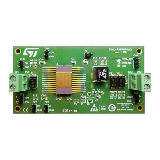
EVAL-RHRPMPOL01 evaluation board of radiation hardened 7 A monolithic
Introduction
This user manual provides an overview of the use of the EVAL-RHRPMPOL01 evaluation board. It has been developed and
optimized for a typical application of the RHRPMPOL01 device, a single phase, step-down monolithic switching regulator with
high precision internal voltage reference and integrated power MOSFETs for synchronous conversion. The regulator
RHRPMPOL01 converts 3 V - 12 V input voltage to 0.8 V - (0.85xVIN) output voltage. The controller is based on a peak current
mode architecture, which ensures a fast load transient response and very stable switching frequency. An embedded integrator
compensates the DC voltage error due to the output voltage ripple.
General features:
•
Input operating voltage: 5.0 V
•
Output voltage: 1.2 V
•
Output current: up to 5 A
•
Enable input voltage: 2.5 V
•
Switching frequency: 500 kHz
•
Output overcurrent protection: 10 A
•
Easy synchronization with 180 ° out-of-phase (up to 2 ICs) management
•
Orderable part number: EVAL-RHRPMPOL01
•
Description: evaluation board of RHRPMPOL01
UM2706 - Rev 1 - April 2020
For further information contact your local STMicroelectronics sales office.
Figure 1.
EVAL-RHRPMPOL01
synchronous switching regulator
UM2706
User manual
www.st.com
Advertisement
Table of Contents

Related Manuals for ST EVAL-RHRPMPOL01


Summary of Contents for ST EVAL-RHRPMPOL01
-
Page 1: Figure 1. Eval-Rhrpmpol01
Introduction This user manual provides an overview of the use of the EVAL-RHRPMPOL01 evaluation board. It has been developed and optimized for a typical application of the RHRPMPOL01 device, a single phase, step-down monolithic switching regulator with high precision internal voltage reference and integrated power MOSFETs for synchronous conversion. -
Page 2: Schematic Diagram
UM2706 Schematic diagram Schematic diagram Figure 2. Schematic diagram CN 2 1.2V 4.7uH VOUT VIN1 VIN2 VOUT VIN3 5.0V VIN4 150uF 150uF 0.1uF 100nF 330uF BOOST BOOT 3.9k 270pF VOUT COMP COMP 8.2K 15pF 4.7nF SSDEL SSDEL/SDA PGOOD 4.7K SYNC SYNC/SCL PGOO D PGOOD... - Page 3 UM2706 Schematic diagram Component Manufacturer Part number / description Value Size 2-pin male strip line 2.54 mm pitch CN1, CN3 Phoenix Contact 2-way PCB terminal 5.08 mm pitch 3-pin male strip line 2.54 mm pitch CN2, CN4,CN5, CN7, CN8, CN9 2-pin male strip line 2.54 mm pitch Coilcraft...
-
Page 4: Input And Output Connections
UM2706 Input and output connections Input and output connections Table 2. Input and output connections Reference/Designator Name Description CN1_1: VIN power CN1_2: GND power CN2_1: VIN sense (s+) VIN_SENSE CN2_2: GND sense (s-) CN3_1: VOUT power VOUT CN3_2: GND power CN4_1: VOUT sense (s+) VOUT_SENSE CN4_2: GND sense (s-) -
Page 5: Connectors
UM2706 Connectors Connectors Figure 3. In/out connectors Connect a power supply between VIN power (CN1_1) and GND power (CN1_2) and a power supply between EN (CN5_1) and GND (CN5_2). The output voltage is present on VOUT pin at the voltage value set by R1 and R2 Connect a multimeter between VIN (S+) (CN2_1) and GND (S-) (CN2_2) for a precise input voltage sensing Connect a multimeter between VOUT (S+) (CN3_1) and GND (S-) (CN3_2) for a precise output voltage... -
Page 6: Board Layout Guidelines
UM2706 Board layout guidelines Board layout guidelines Guidelines The DC-DC converter area is very sensitive, and it is necessary to pay attention to the layout of this part. This is because the DC-DC converter generates GND noise that can get coupled with surrounding ground reducing the sensitivity and high-frequency components can disturb the RF part of the system. -
Page 7: Ground Plane
UM2706 Ground plane Figure 5. 4-layer board Ground plane Any switch mode power supply requires a good PCB layout in order to achieve the maximum performance. Component placement, GND trace routing and width are the major issues. Basic rules commonly used for DC-DC converters for good PCB layout should be followed. -
Page 8: Capacitor Placing
UM2706 Capacitor placing Figure 7. Ground plane assignment Figure 8. Ground plane assignment 2 Capacitor placing Particular care has to be taken in the placement of the supply voltage filtering capacitors. It is, in fact, important to ensure efficient filtering by placing these capacitors as close as possible to their dedicated pins on the VIN,VREF,VFB,VDD and VDRIVE. -
Page 9: Inductor Placing
UM2706 Inductor placing Inductor placing The DC-DC converter inductor has to be placed as close as possible to the LX pin, with short and thick traces. This should minimize resistive parasitic effects, and increase system efficiency. Figure 10. Inductor placing Vias placing It is crucial to connect very well the ground of the exposed pad of the FLAT28 to the ground on the application board. -
Page 10: Feedback Voltage
UM2706 Feedback voltage Connect all the ground metallization and/or layers with as many vias as possible. The vias should be located at minimum keepout distance, in order to minimize resistive and inductive parasitic effects. Figure 12. Vias placing 2 Feedback voltage VFB is generated by a precision voltage divider (use of low tolerance resistors is recommended). -
Page 11: Thermal Aspects
UM2706 Thermal aspects Figure 13. Feedback voltage Thermal aspects The RHRPMPOL01 power dissipation inside the IC is mainly due to the DC-DC integrated MOSFETs power loss. The heat generated due to this power dissipation level requires a suitable heatsink to keep the junction temperature below the overtemperature protection threshold at the rated ambient temperature. -
Page 12: Figure 14. Thermal Aspects
UM2706 Thermal aspects Figure 14. Thermal aspects UM2706 - Rev 1 page 12/19... -
Page 13: Board Layout
UM2706 Board layout Board layout Figure 15. Assembly layer Figure 16. Top layer UM2706 - Rev 1 page 13/19... -
Page 14: Figure 17. Mid Layer1
UM2706 Board layout Figure 17. Mid layer1 Figure 18. Mid layer2 UM2706 - Rev 1 page 14/19... -
Page 15: Figure 19. Bottom Layer
UM2706 Board layout Figure 19. Bottom layer UM2706 - Rev 1 page 15/19... -
Page 16: Revision History
UM2706 Revision history Table 3. Document revision history Date Version Changes 14-Apr-2020 Initial release. UM2706 - Rev 1 page 16/19... -
Page 17: Table Of Contents
UM2706 Contents Contents Schematic diagram ..............2 Input and output connections . - Page 18 EVAL-RHRPMPOL01 ........
- Page 19 ST’s terms and conditions of sale in place at the time of order acknowledgement. Purchasers are solely responsible for the choice, selection, and use of ST products and ST assumes no liability for application assistance or the design of Purchasers’...
Need help?
Do you have a question about the EVAL-RHRPMPOL01 and is the answer not in the manual?
Questions and answers