
Related Manuals for Star Lake OXY5363A


Summary of Contents for Star Lake OXY5363A
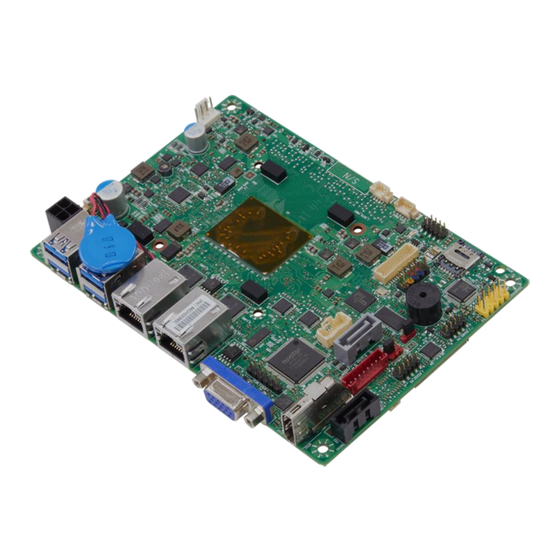
- Page 1 OXY5363A 3.5" SBC Form Factor Intel® Apollo Lake Processor User’s Manual Revision Date: Feb.14.2022...
-
Page 2: Safety Information
OXY5323A User’s Manual Revision Date: Feb.14.2022 Safety Information Electrical safety To prevent electrical shock hazard, disconnect the power cable from the electrical outlet before relocating the system. When adding or removing devices to or from the system, ensure that the power cables for the devices are unplugged before the signal cables are connected. -
Page 3: Electrical Safety
OXY5323A User’s Manual Revision Date: Feb.14.2022 Revision History Date (yyyy/mm/dd) Changes Revision V1.0 2021/09/08 First release V1.1 2022/02/14 Standard Compliance Packing List Q’ty Item Description OXY5323A IEC-61850-3, IEEE-1613 1U Computer Driver CD+ User’s manual If any of the above items is damaged or missing, please contact your local distributor. -
Page 4: Table Of Contents
OXY5323A User’s Manual Revision Date: Feb.14.2022 Table of Contents Safety Information……………………………………………………………………………… Electrical safety ......................... 1 Operation safety ........................1 Statement ..........................1 Revision History .......................... 2 Packing list ........................... 2 Ordering information……………………………….……………………………………………………………………………….. Chapter 1: Product Information ....................7 1.1 Block Diagram ........................7 1.2 Specifications ........................ - Page 5 OXY5323A User’s Manual Revision Date: Feb.14.2022 2.13 Serial Port .......................... 17 2.14 AT/ATX,CMOS,Msata header in silkscreen/feature ............19 2.15 SATA power 1.25mm cable pin header ................19 2.16 ATX power 4P/DC power 4.2mm pin header ..............20 2.17 Thermal Management and Fan Control ................21 2.18 CPU Fans ...........................
- Page 6 OXY5323A User’s Manual Revision Date: Feb.14.2022 3.10 Platfrom Trust Technology ................... 57 3.11 Chipset ........................... 59 3.12 Security .......................... 65 3.12.1 HDD Security Configuration ................... 67 3.12.2 Secure Boot Mode ....................69 3.12.3 Key Managerment ....................71 3.13 Boot ..........................76 3.14 Save &...
-
Page 7: Block Diagram
OXY5323A User’s Manual Revision Date: Feb.14.2022 Chapter 1 : Production Introduction 1.1 Block Diagram... -
Page 8: Specifications
OXY5323A User’s Manual Revision Date: Feb.14.2022 1.2 Specifications System Intel® Apollo Lake-M N3350/N4200 Processor Intel® Apollo Lake-I E3930 Processor Memory type DDR3L 1866MHz, 1 x 204pin SO-DIMM, Max. 8GB (Non-ECC) Chipset Intel® SoC Integrated Intel® HD Graphics Graphics Ethernet 2 x Intel® I210-IT Giga LAN Realtek®... -
Page 9: Chapter 1: Product Information
OXY5323A User’s Manual Revision Date: Feb.14.2022 1 x 4-pin CPU Fan Header Power 1 x 8~24V ATX Power Connector, 1 x AT/ATX Mode Select Jumper Others 1 x CMOS Jumper Power Requirement Power Input 8~24V Wide Range DC Input w/4-pin ATX connector (Pitch: 4.2mm) Environmental Operating -20 to 70°C (Optional -40 to 85°C) -
Page 10: Board Placement
OXY5323A User’s Manual Revision Date: Feb.14.2022 1.3 Board Placement... -
Page 11: Chapter 2: Jumper Setting And Pin Definition
OXY5323A User’s Manual Revision Date: Feb.14.2022 Chapter 2 : Jumpers and Connectors 2.1 FRONT_PANEL1 (JLVDS1) LVDS panel pin out define DEFINITION DEFINITION Minus signal of odd Minus signal of odd channel 0 (LVDS) channel 0 (LVDS) Plus signal of odd Plus signal of odd channel 0 (LVDS) channel 0 (LVDS) - Page 12 OXY5323A User’s Manual Revision Date: Feb.14.2022 2.2 eDP1 Pin out define Signal Pin Signal NC_ Reserved LCD_VCC High-speed _GND LCD_ Self _ Test-or-NC Lane3_N(DDPD_[3]N) LCD_GND Lane3_P(DDPD_[3]P) LCD_GND High-speed_ GND LCD_GND Lane2_N(DDPD_[2]N) LCD_GND Lane2_P(DDPD_[2]P) HDP(DDPD_HPD) High-speed_ GND BKLT_GND Lane1_N(DDPD_[1]N) BKLT_GND Lane1_P(DDPD_[1]P) BKLT_GND High-speed_ GND BKLT_GND...
- Page 13 OXY5323A User’s Manual Revision Date: Feb.14.2022 LCD_PS1 : Panel LCD voltage selection header pin-out Signal Description 3.3V No pin Pins 2&4: Jumper position for 3.3V 3.3V option 3.3V (Default) 12V option Pins 6&4: Jumper position for 5V Send voltage to LCD_VCC connector No pin...
-
Page 14: Audio Pin Out Define
OXY5323A User’s Manual Revision Date: Feb.14.2022 2.3 FPAUDIO2 Audio Pin out define Sense2_Ret Port2L Key(no pin) Sense _Send Sense1_Ret Port2R Presence# Port1R Ground Port1L Pin Assignment Pin Assignment MIC2 L (Microphone 2 Left) AGND (Analog Ground) MIC2 R (Microphone 2 Right) AVCC (Analog VCC Power) MIC2_JD (Microphone 2 Jack FRO-R (Front Right) -
Page 15: Sata
OXY5323A User’s Manual Revision Date: Feb.14.2022 2.5 SATA SATA PORT0: This is optional port from mini PCI-E and SATA0 Connector One fully-shrouded right angle internal SATA gen 3 ports (colored GREY) SATA PORT1 one fully- Note: All SATA must be compliant with the Serial ATA Revision 3.0 Specification, as noted in the Reference Documentation section. -
Page 16: Usb
OXY5323A User’s Manual Revision Date: Feb.14.2022 2.8 USB Front panel USB header pin-out define (FP_USB1) Pin Signal Signal FP_USB1 +5V DC +5V DC Data (negative) Data (negative) Data (positive) Data (positive) Ground Ground Key (no pin) No Connect Rear USB3.0 I/O port (J5/J10) Mating J5/J10 Signal Name... -
Page 17: Pci Express Expansion Slots
OXY5323A User’s Manual Revision Date: Feb.14.2022 2.9 PCI Express Expansion Slots Board’s PCI Express slot(s) must be PCI Express Specification v2.0 compliant and compatible with PCI Express v2.0 and v1.1 add-in cards. PCI Express x16 slot must be compatible with x16/x8/x4/x1 PCI Express add-on cards. PCIe x16 slot’s retention mechanism must be consistent across Intel desktop boards. -
Page 18: Expansion Slots Layout
OXY5323A User’s Manual Revision Date: Feb.14.2022 2.10 Expansion Slot Layout Slot Configuration Electrical Physical Connector Color M.2 key M socket M.2 Key E socket Black PCI Express 3.0 x1 Mini PCIE Black 2.11 Front Panel Pin out define (JS2) PWR_LED ON / OFF RESET HDD_LED... -
Page 19: Miapi Feature
OXY5323A User’s Manual Revision Date: Feb.14.2022 2.12 J_MiAPI_1 Pin out define Signal Name Signal Name MAPI_GPIO1 MAPI_GPIO2 MAPI_GPIO6 MAPI_GPIO3 MAPI_GPIO7 MAPI_GPIO4 MAPI_GPIO8 MAPI_GPIO5 MAPI_GPIO9 Watchdog Timer MAPI_GPIO10 Power Button SMB_MAIN_DATA UART_TX SMB_MAIN_CLK UART_RX 5VSB 2.13 Serial Port J_RS485_P4, J_RS232_P2 Serial port header pin out define... - Page 20 OXY5323A User’s Manual Revision Date: Feb.14.2022 RS232_P1P3 Serial port header pin out define Signal Signal RS485/RS422/RS232 feature: RS232 RS232 DCD (Data Carrier RXD# (Receive Data) Detect) DTR (Data Terminal TXD# (Transmit Data) Ready) Ground DSR (Data Set Ready) RTS (Request To CTS (Clear To Send) Send) RI (Ring Indicator)
-
Page 21: At/Atx,Cmos,Msata Header In Silkscreen/Feature
OXY5323A User’s Manual Revision Date: Feb.14.2022 2.14 AT/ATX, CMOS , mSATA header in silkscreen / feature (J_AT_CMOS1) pin out define JUMPER J_AT_CMOS1 (1-2) Clear CMOS (1-3) Normal (4-6) (6-8) (5-7) PCIE (5-7) NA mSATA CMOS clear JUMPER (1-2) (1-3) Normal: 1-3 Clear CMOS Clear CMOS Normal... -
Page 22: Atx Power 4P/Dc Power 4.2Mm Pin Header
OXY5323A User’s Manual Revision Date: Feb.14.2022 2.16 ATX power 4P/DC power 4.2mm pin out define J_PW4P_1 signal Power 8V~24V Power 8V~24V... -
Page 23: Thermal Management And Fan Control
OXY5323A User’s Manual Revision Date: Feb.14.2022 2.17 Thermal Management and Fan Control Nuvoton NCT6104D SuperIO: backup alternate solution as it leverages existing hardware in the designs, but software infrastructure must be put in place to support this solution. Regardless of solution chosen, BIOS/driver/tools support and subsystem validation is required, even if solution is not needed by pilot. -
Page 24: Cpu Fans
OXY5323A User’s Manual Revision Date: Feb.14.2022 2.18 CPU Fans Processor fan header (J20) :... -
Page 25: Fan Header Requirements
OXY5323A User’s Manual Revision Date: Feb.14.2022 2.19 Fan Header Requirements The below requirements must be met for the 4- Closed loop fan speed control via the FANPWM0 signal routed to pin- Locate closest to the CPU as required by the CDPG boxed CPU Chapter 3 : BIOS Specification This chapter provides information about how to set up BIOS and use BIOS menu items to adjust basic function settings. - Page 26 OXY5323A User’s Manual Revision Date: Feb.14.2022...
- Page 27 OXY5323A User’s Manual Revision Date: Feb.14.2022...
-
Page 28: Advanced Page
OXY5323A User’s Manual Revision Date: Feb.14.2022 3.2 ADVANCED PAGE... - Page 29 OXY5323A User’s Manual Revision Date: Feb.14.2022...
- Page 30 OXY5323A User’s Manual Revision Date: Feb.14.2022...
- Page 31 OXY5323A User’s Manual Revision Date: Feb.14.2022...
-
Page 32: Intel
OXY5323A User’s Manual Revision Date: Feb.14.2022 3.2.1 INTEL(R) I210 GIGABIT NETWORK CONNECTION – 00:22:4D:4D:00:01... - Page 33 OXY5323A User’s Manual Revision Date: Feb.14.2022...
-
Page 34: Nic Configuration
OXY5323A User’s Manual Revision Date: Feb.14.2022 3.2.2 NIC CONFIGURATION... - Page 35 OXY5323A User’s Manual Revision Date: Feb.14.2022...
-
Page 36: Intel
OXY5323A User’s Manual Revision Date: Feb.14.2022 3.2.3 INTEL(R) I210 GIGABIT NETWORK CONNECTION – 00:22:4D:4D:00:02... - Page 37 OXY5323A User’s Manual Revision Date: Feb.14.2022...
-
Page 38: Nic Configuration
OXY5323A User’s Manual Revision Date: Feb.14.2022 3.2.4 NIC CONFIGURATION... -
Page 39: Driver Health
OXY5323A User’s Manual Revision Date: Feb.14.2022 3.3DRIVER HEALTH... -
Page 40: Intel® Pro/1000 7.3.20 Pcie
OXY5323A User’s Manual Revision Date: Feb.14.2022 3.3.1 INTEL(R) PRO/1000 7.3.20 PCI-E... - Page 41 OXY5323A User’s Manual Revision Date: Feb.14.2022...
-
Page 42: Trusted Computing
OXY5323A User’s Manual Revision Date: Feb.14.2022 3.4 TRUSTED COMPUTING... - Page 43 OXY5323A User’s Manual Revision Date: Feb.14.2022...
-
Page 44: Smart Settings
OXY5323A User’s Manual Revision Date: Feb.14.2022 3.5 SMART SETTINGS... -
Page 45: Nct6116D Super Io Configuration
OXY5323A User’s Manual Revision Date: Feb.14.2022 3.6 NCT6116D SUPER IO CONFIGURATION... - Page 46 OXY5323A User’s Manual Revision Date: Feb.14.2022...
- Page 47 OXY5323A User’s Manual Revision Date: Feb.14.2022...
-
Page 48: S5 Rtc Wake Settings
OXY5323A User’s Manual Revision Date: Feb.14.2022 3.7 S5 RTC WAKE SETTINGS (NO FUNCTION WHEN DEEPSX POWER POLICIES ENABLED) - Page 49 OXY5323A User’s Manual Revision Date: Feb.14.2022...
- Page 50 OXY5323A User’s Manual Revision Date: Feb.14.2022...
-
Page 51: Cpu Configuration
OXY5323A User’s Manual Revision Date: Feb.14.2022 3.8 CPU CONFIGURATION... - Page 52 OXY5323A User’s Manual Revision Date: Feb.14.2022...
- Page 53 OXY5323A User’s Manual Revision Date: Feb.14.2022...
- Page 54 OXY5323A User’s Manual Revision Date: Feb.14.2022...
- Page 55 OXY5323A User’s Manual Revision Date: Feb.14.2022...
- Page 56 OXY5323A User’s Manual Revision Date: Feb.14.2022...
-
Page 57: Network Stack Configuration
OXY5323A User’s Manual Revision Date: Feb.14.2022 3.9 NETWORK STACK CONFIGURATION... - Page 58 OXY5323A User’s Manual Revision Date: Feb.14.2022...
-
Page 59: Platfrom Trust Technology
OXY5323A User’s Manual Revision Date: Feb.14.2022 3.10 PLATFROM TRUST TECHNOLOGY... - Page 60 OXY5323A User’s Manual Revision Date: Feb.14.2022...
-
Page 61: Chipset
OXY5323A User’s Manual Revision Date: Feb.14.2022 3.11 CHIPSET... - Page 62 OXY5323A User’s Manual Revision Date: Feb.14.2022...
- Page 63 OXY5323A User’s Manual Revision Date: Feb.14.2022...
- Page 64 OXY5323A User’s Manual Revision Date: Feb.14.2022...
- Page 65 OXY5323A User’s Manual Revision Date: Feb.14.2022...
- Page 66 OXY5323A User’s Manual Revision Date: Feb.14.2022...
-
Page 67: Security
OXY5323A User’s Manual Revision Date: Feb.14.2022 3.12 SECURITY... - Page 68 OXY5323A User’s Manual Revision Date: Feb.14.2022...
-
Page 69: Hdd Security Configuration
OXY5323A User’s Manual Revision Date: Feb.14.2022 3.12.1 HDD SECURITY CONFIGURATION... - Page 70 OXY5323A User’s Manual Revision Date: Feb.14.2022...
-
Page 71: Secure Boot Mode
OXY5323A User’s Manual Revision Date: Feb.14.2022 3.12.2 SECURE BOOT MODE... - Page 72 OXY5323A User’s Manual Revision Date: Feb.14.2022...
-
Page 73: Key Managerment
OXY5323A User’s Manual Revision Date: Feb.14.2022 3.12.3 KEY MANAGERMENT... - Page 74 OXY5323A User’s Manual Revision Date: Feb.14.2022...
- Page 75 OXY5323A User’s Manual Revision Date: Feb.14.2022...
- Page 76 OXY5323A User’s Manual Revision Date: Feb.14.2022...
- Page 77 OXY5323A User’s Manual Revision Date: Feb.14.2022...
-
Page 78: Boot
OXY5323A User’s Manual Revision Date: Feb.14.2022 3.13 BOOT... - Page 79 OXY5323A User’s Manual Revision Date: Feb.14.2022...
- Page 80 OXY5323A User’s Manual Revision Date: Feb.14.2022...
- Page 81 OXY5323A User’s Manual Revision Date: Feb.14.2022...
-
Page 82: Save & Exit
OXY5323A User’s Manual Revision Date: Feb.14.2022 3.14 SAVE & EXIT... - Page 83 OXY5323A User’s Manual Revision Date: Feb.14.2022...
Need help?
Do you have a question about the OXY5363A and is the answer not in the manual?
Questions and answers