Table of Contents
Advertisement
Quick Links
Advertisement
Table of Contents

Related Manuals for Microchip Technology HV7358DB1


Summary of Contents for Microchip Technology HV7358DB1
- Page 1 HV7358DB1 User’s Guide 2020 Microchip Technology Inc. DS50002951A...
- Page 2 Technology, and Symmcom are registered trademarks of Microchip Technology Inc. in other countries. GestIC is a registered trademark of Microchip Technology Germany II GmbH & Co. KG, a subsidiary of Microchip Technology Inc., in other countries. All other trademarks mentioned herein are property of their respective companies.
-
Page 3: Table Of Contents
1.1 Introduction ..................... 9 1.2 Features ....................... 10 1.3 Device summary ................... 10 1.4 Functional Description .................. 12 1.5 What the HV7358DB1 ADM00732 Kit Includes ........... 12 Chapter 2. HV7358 Overview..................13 2.1 Getting Started ..................... 13 2.2 USB Driver Installation ................. 13 2.3 HV7358DB1 GUI Installation ................ - Page 4 Appendix D. HV7358 GUI Parameter and Default ............75 D.1 HV7358 GUI Parameter Limits and Default Page-1 ........75 D.2 HV7358DB1 GUI Parameter Initial Value and Limits Page-2 ...... 76 D.3 HV7358DB1 GUI Parameter Initial Value and Limits Page-3 ...... 77 Worldwide Sales and Service ..................78...
-
Page 5: Preface
• Customer Support • Document Revision History DOCUMENT LAYOUT This document describes how to use the HV7358DB1 User’s Guide as a development tool. The document is organized as follows: • – Important information about the HV7358DB1 Chapter 1. “HV7358 Overview”... -
Page 6: Conventions Used In This Guide
HV7358DB1 User’s Guide • – Shows Appendix A. “HV7835DB1 and MUPB002 Schematics and Layouts” the schematics and layouts for the HV7358DB1 and MUP002. • – Lists the parts used to build the Appendix B. “Bill of Materials (BOM)” HV7358DB1 Evaluation Board. -
Page 7: Recommended Reading
Preface RECOMMENDED READING This user’s guide describes how to use the HV7358DB1 Evaluation Board. The follow- ing Microchip document is available and recommended as a supplemental reference resource. • HV7358 Data Sheet – “16-Channel, 3-Level HV Ultrasound Transmitter with Built-In Transmit Beamformer” (20005918) THE MICROCHIP WEBSITE Microchip provides online support via our website at www.microchip.com. - Page 8 HV7358DB1 User’s Guide NOTES: 2020 Microchip Technology Inc. DS50002951A-page 8...
-
Page 9: Chapter 1. Hv7358 Overview
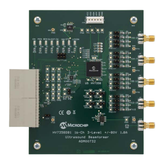
USER’S GUIDE Chapter 1. HV7358 Overview INTRODUCTION The HV7358DB1 Evaluation Board (ADM00732), working with the MUPB002 (ADM00900), provides a demonstration platform to test and characterize the HV7358. The HV7358 is a 16-channel, 3 level, 80V, 1.6A ultrasound transmit beamformer. It is ±... -
Page 10: Features
• On-board SPI EEPROM for the ultrasound demonstration board ID • Test points for convenient measurement • On-board 5V and 3.3V voltage supplies available for user DEVICE SUMMARY The HV7358DB1 Evaluation Board contains the following Microchip products: • HV7358: 16-Channel, 3-Level, 80V, 1.6A Ultrasound TX Beamformer ±... - Page 11 Open-Drain Output to J5 and J12 to MUPB002 Floating Gate Driver Voltage Regulators Built-in Floating Regulators in HV7358 PCB Board Dimension 127 x 102 mm (5.0 x 4.0 Inch) FIGURE 1-2: HV7358DB1 Block Diagram. 2020 Microchip Technology Inc. DSXXXXXX-page 11...
-
Page 12: Functional Description
GUI software to automatically identify the demonstration board ID. All of the 16 TX outputs are accessible at test points on the HV7358DB1. There are also four SMA connectors on the board that can be connected to the TX outputs via jumper shorting plugs. -
Page 13: Chapter 2. Hv7358 Overview
Chapter 2. HV7358DB1 Software Installation GETTING STARTED The HV7358DB1 Evaluation Board requires the use of the MUPB002 board, PC GUI software and multiple voltage rails power supply for the full functional demonstration. Both the MPUB002 board and the HV7358DB1 are required to test the boards. - Page 14 HV7358DB1 User’s Guide FIGURE 2-1: View of “Device Manager” Screen. FIGURE 2-2: Close-up of “Bridge device” with Error. 2020 Microchip Technology Inc. DS50002951A-page 14...
- Page 15 HV7358DB1 Software Installation 6. A pop-up window will open as shown in Figure 2-3 below. Choose “Update driver” and click on it. FIGURE 2-3: “Update driver” Pop-up Window. 2020 Microchip Technology Inc. DS50002951A-page 15...
- Page 16 Figure 2-4 will appear. Choose “Browse my computer for driver software”. FIGURE 2-4: Driver Search Window. 8. The following window will open. Click on the Browse button. FIGURE 2-5: Driver Browse Choice Window. 2020 Microchip Technology Inc. DS50002951A-page 16...
- Page 17 Browse to “Drivers” Folder Window. The window in Figure 2-7 will appear. The path shown will point to the drivers used by the MPLABConnect tool. 10. Click the Next button. FIGURE 2-7: Browse for Drivers Screen. 2020 Microchip Technology Inc. DS50002951A-page 17...
- Page 18 FIGURE 2-8: Install Verification Screen. 12. After successful installation, the window shown in Figure 2-9 will appear. This verifies that you have installed the USB driver. FIGURE 2-9: USB Driver Installation Verification Screen. 2020 Microchip Technology Inc. DS50002951A-page 18...
-
Page 19: Hv7358Db1 Gui Installation
HV7358DB1 Software Installation HV7358DB1 GUI INSTALLATION Download the MUPB002/HV7358DB1 GUI Installation tool from the Microchip website. The HV7358 GUI program will require about 2.6 MB hard drive space. 1. Double click on the file named, MUPB002 – HV7358 GUI Setup. The window in Figure 2-10 below will pop up. - Page 20 5. The next window, shown in Figure 2-13, confirms that you are ready to install the HV7358 GUI. If so, click Next; otherwise, you can go back and make changes or Cancel. FIGURE 2-13: Installation Confirmation. 2020 Microchip Technology Inc. DS50002951A-page 20...
- Page 21 FIGURE 2-15: Installation Complete Window. The icon below in Figure 2-16 will be left on your desktop. Double click to open the HV7358 GUI. The GUI Installation is complete. FIGURE 2-16: HV7358 GUI Icon. 2020 Microchip Technology Inc. DS50002951A-page 21...
- Page 22 HV7358DB1 User’s Guide NOTES: 2020 Microchip Technology Inc. DS50002951A-page 22...
-
Page 23: Chapter 3. Hv7358Db1 Gui Operation
To operate the HV7358DB1, the following steps must be completed: 1. Connect J1 and J2 of the MPUB002 board to J5 and J12 of the HV7358DB1. 2. Connect a USB cable from the lower male Micro-B connector (J7) on the MPUB002 board to any USB connector on your PC. -
Page 24: Hv7358Db1 Power Supply Requirements
HV7358DB1 User’s Guide HV7358DB1 POWER SUPPLY REQUIREMENTS Connect all power supplies to the HV7358DB1 power supply connector (J10). The voltage and current requirements can be found in Table 3-2 below. Leave the power supplies turned off. TABLE 3-2: J10 POWER SUPPLY CONNECTION INFORMATION... -
Page 25: Mupb002 And Gui/Usb Programming
HV7358DB1 GUI Operation MUPB002 AND GUI/USB PROGRAMMING Open and run the GUI by double clicking the HV7358DB1 icon. The GUI will open showing the following screen: FIGURE 3-1: Full GUI Screen. At the bottom left hand corner, there should be the “USB Status: Connected” note, as... - Page 26 In the upper left corner there is a “Demo Board Info” box, as shown in Figure 3-4 below. Click on the Check DB ID button. An HV7358DB1 revision number and an FPGA code version number should be shown. If the USB status is “Connected” and the “Demo Board Info” is shown per above, then the GUI has successfully connected to the MUPB002 board.
- Page 27 These switches have a 5 mA capability and are meant to discharge the bypass caps only. The supplies need to be turned off before activating the discharge switches. 2020 Microchip Technology Inc. DS50002951A-page 27...
- Page 28 “Power Within Limit”; otherwise, it will read “Power Outside Limit” and the Start button will be disabled. For CW mode, 100% will be used for the duty cycle. FIGURE 3-7: Mode and Power Dissipation Window. 2020 Microchip Technology Inc. DS50002951A-page 28...
- Page 29 In CW mode, the PLL function cannot be used. Therefore, PEN and the PLL are disabled. Choose the frequency by clicking on the appropriate box, then click on the Set CLK + FPGA button. PEN = 0 PEN = 1 FIGURE 3-8: Transmit Clock Frequency Window. 2020 Microchip Technology Inc. DS50002951A-page 29...
- Page 30 C settings or write new ones. The default settings can be used for most applications. The HV7358DB1 is the slave and the HV7358 GUI is the master. The slave address (‘111’ by default) can be changed by adding jumpers on J28, J30 and J31.
- Page 31 Waveform 0 through 3. FIGURE 3-11: “Waveform Definition” Box. Knowing the maximum pulse width, calculate TGW. Enter into the TGW box for each waveform. Enter into the RPC box for each waveform. See Figure 3-11. 2020 Microchip Technology Inc. DS50002951A-page 31...
- Page 32 C register. The bits are used in determining the F frequency when in PLL mode. See Section 3.4.4 “Transmit Clock Frequency Configuration Window”. TABLE 3-11: FREQUENCY MULTIPLIER N[2:0] in GUI N[2:0] in HV7358 2020 Microchip Technology Inc. DS50002951A-page 32...
- Page 33 Table 3-12. TABLE 3-12: TRDLY Decimal 3.4.8.6 PSEL BIT PSEL is the I C bit that determines if PLLEN or PEN controls the PLL enable. TABLE 3-13: PSEL EFFECT PSEL Controlling Signal PLLEN 2020 Microchip Technology Inc. DS50002951A-page 33...
- Page 34 V(x)UV BITS These five bits are output flags. They can be read, but not written. They signal an undervoltage on their respective power supply. V(x)UV can stand for: VNFUV, VPFUV, VPLLUV, VDDUV or VLLUV. 2020 Microchip Technology Inc. DS50002951A-page 34...
- Page 35 SPIBC FOR SPISEL = 1 SPIBC Disabled Enabled 3.4.8.17 Manually Read BUTTON The Manually Read button will read and display the current values of the I C registers. FIGURE 3-12: C Parameter Read Back Window. 2020 Microchip Technology Inc. DS50002951A-page 35...
- Page 36 TLPx and TLNx bits. The pulse for each channel will be: EQUATION 3-9: POSITIVE PULSE WIDTH = (P – TLPx) x (1/F EQUATION 3-10: NEGATIVE PULSE WIDTH = (P – TLNx) x (1/F 2020 Microchip Technology Inc. DS50002951A-page 36...
-
Page 37: Running The Hv7358Db1
2. Turn on the power supplies, observing the power-up sequence in Table 3-3. 3. Click on the Start button. The HV7358DB1 is now running. STOPPING THE HV7358DB1 1. Click on the Stop button. 2. Power down the power supplies, observing the power-down sequence in Table 3-3. -
Page 38: Sample Waveform
HV7358DB1 User’s Guide SAMPLE WAVEFORM A sample of the waveform generation is shown in Figure 3-15. FIGURE 3-15: Sample Waveform from Multiple Channels of the HV7358. 2020 Microchip Technology Inc. DS50002951A-page 38... -
Page 39: Chapter 4. Mupb002 Fpga Configuration
Chapter 4. MUPB002 FPGA Configuration INTRODUCTION The MUPB002 board connects to and controls the HV7358DB1. It connects to the host PC and interfaces with the GUI. The MUPB002 is preprogrammed and ready for immediate use. However, if changes in the code are required, the directions below will allow changes to the configuration. -
Page 40: Software Execution
4. Right click on top of the “Right click to Add Device or Initialize JTAG chain” statement. FIGURE 4-2: iMPACT Window. 5. Choose “Add Xilinx Device…” from the menu and click. FIGURE 4-3: Xilinx Setup Window. 2020 Microchip Technology Inc. DS50002951A-page 40... - Page 41 It shows an external block diagram of the FPGA (xc6slx25). Now we will choose the Flash memory that we want to configure. 7. Right click on the “SPI/BPI?” statement on top of the FPGA symbol. FIGURE 4-5: SPI/BPI Window. 2020 Microchip Technology Inc. DS50002951A-page 41...
- Page 42 The window in Figure 4-8 will appear. 11. Select “S25FL128S” for the 128 MB Flash memory (U15) installed on the MUPB002 board. 12. Click the OK button. FIGURE 4-8: Select Attached SPI/BPI Window. 2020 Microchip Technology Inc. DS50002951A-page 42...
- Page 43 13. There is a FLASH button in the upper right. Click on it. FIGURE 4-9: FLASH Button. The FLASH button will turn green as shown in Figure 4-10. 14. Click on the green FLASH button. FIGURE 4-10: Green FLASH Button. 2020 Microchip Technology Inc. DS50002951A-page 43...
- Page 44 15. Click the OK button. FIGURE 4-11: Device Programming Properties Window. The FPGA will be programmed. This may take over a minute. When completed, the window in Figure 4-12 will appear. FIGURE 4-12: Complete Window. 2020 Microchip Technology Inc. DS50002951A-page 44...
-
Page 45: Conclusion
MUPB002 FPGA Configuration CONCLUSION A procedure to program the MUPB002 FPGA for use with the HV7358DB1 has been presented. This procedure with different file names can be used to program the MUPB002 for different Microchip ultrasound transmitters. 2020 Microchip Technology Inc. - Page 46 HV7358DB1 User’s Guide NOTES: 2020 Microchip Technology Inc. DS50002951A-page 46...
-
Page 47: Chapter 5. Pcb Design And Layout Techniques
Chapter 5. PCB Design and Layout Techniques INTRODUCTION The PCB layout techniques are a very important part of the ultrasound system design. The HV7358DB1 generates high-voltage, high-current, high-frequency and high-speed pulses. Proper PCB layout is required to optimize the waveforms. 5.1.1... - Page 48 These EMI problems can usually be avoided with proper design of the return current path. 2020 Microchip Technology Inc. DS50002951A-page 48...
-
Page 49: Appendix A. Hv7835Db1 And Mupb002 Schematics And Layouts
HV7358DB1 USER’S GUIDE Appendix A. HV7835DB1 and MUPB002 Schematics and Layouts INTRODUCTION This appendix contains the following schematics and layouts for the HV7358DB1 and MUPB002: • HV7358DB1 – Schematic • MUPB002 Schematic – Top Block Diagram • MUPB002 Schematic – Demo Board Connectors •... -
Page 50: Hv7358Db1 - Schematic
HV7358DB1 – SCHEMATIC SLEEP LCKD (+5V) OTPN D17B LCKD (+2.5V) MCP1727-2502E/SN 2.2μ 10V C123 C125 SENSE C122 C124 C126 1μ 10V C121 DELAY OUT1 SHDN 1.27k 1.27k D17A 2.2μ 10V 1μ 100V 1μ 100V 2.2μ 10V TP17 2.2μ 10V 2.5K 1W... -
Page 51: Mupb002 Schematic - Top Block Diagram
MUPB002 SCHEMATIC – TOP BLOCK DIAGRAM 3V3_VDD To connector for programming the SPI Flash for FPGA program. GND_D HDR-2.54 Male 2x4 Demo Board connectors.SchDoc HDR-2.54 Male 1x4 SPI_MISO MISO SPI_MOSI MOSI SPI_SCLK DBID_EEPROM_CS SCLK DB_MEMORY_CS DBID_EEPROM_CS FPGA_FLASH_CS MUPB_FLASH_CS PLUG_DETECT PLUG_DETECT SPI Flash for FPGA configuration.SchDoc MISO MOSI... -
Page 52: Mupb002 Schematic - Demo Board Connectors
MUPB002 SCHEMATIC – DEMO BOARD CONNECTORS 3V3_VDD 3V3_VDD 4.7k 0402 C133 0.1 µF 0402 GND_D 3V3_VDD SCLK PWR5V0 PWR5V0 PWR3V3 SN74LVC1G126 C131 C132 33 µF GND_D 0.1 µF 33 μF 0.1 µF 0.1 µF 33 μF TANT-B 0603 TANT-B 0603 0603 TANT-B 4.7k... -
Page 53: Mupb002 Schematic - Fpga
MUPB002 SCHEMATIC – FPGA CTRL_SDI When the FPGA is loading its firmware from the SPI IO_L83N_VREF_3 CTRL_SDI IO_L1P_A25_1 CTRL_CSB Flash, the FPGA genetaes the SCLK. (The FPGA is IO_L83P_3 CTRL_CSB IO_L1N_A24_VREF_1 the SPI bus master.) IO_L55N_M3A14_3 IO_L29P_A23_M1A13_1 IO_L55P_M3A13_3 IO_L29N_A22_M1A14_1 The USB to SPI bridge generates the SCLK, when it's IO_L54N_M3A11_3 IO_L30P_A21_M1RESET_1 sending commands to the FPGA. -
Page 54: Mupb002 Schematic - Spi Flash For Fpga Configuration
MUPB002 SCHEMATIC – SPI FLASH FOR FPGA CONFIGURATION MOSI SCLK MISO 0402 3V3_VDD Partial list of SPI Flash ICs which we can use with 3V3_VDD 3V3_VDD 3V3_VDD Spartan-6: S25FL127SABMFI101, S25FL127SABMFV101. C138 2.43k 0.1 µF 0402 0402 0402 0402 S25FL127SABMFI101 GND_D FLASH_CS SO/SIO1 HOLD/SIO3... -
Page 55: Mupb002 Schematic - Programmable Clock
MUPB002 SCHEMATIC – PROGRAMMABLE CLOCK USB 2.0 MICRO-B FEMALE USB_5V USB_N MBR0540T1G USB_P 4.7 μF 4.7 μF 1206 1206 GND_D GND_D GND_D 330R 0.1 µF 0603 0603 3V3_VDD GND_D GND_D 3V3_VDD 100k 0402 C134 Upstream 0.1 µF USB_P FLEX_USBUP_DP/PRT_DIS_P0 USB_N 0402 FLEX_USBUP_DM/PRT_DIS_M0 0402... -
Page 56: Mupb002 Schematic - Fpga Decoupling Capacitors
MUPB002 SCHEMATIC – FPGA DECOUPLING CAPACITORS USB 2.0 MICRO-B FEMALE MBR0540T1G 4.7 μF 4.7 μF 1206 1206 GND_D GND_D GND_D 330R 0.1 µF 0603 0603 GND_D GND_D 3V3_VDD 1V2_VCCINT MCP172X ADJ DFN-8 MCP172X ADJ DFN-8 Via_2.5x1.5 69.8k Via_2.5x1.5 SHDN 0603 10 μF 0.1 μF DELAY... -
Page 57: Hv7358Db1 - Top Silk
HV7358DB1 and MUPB002 Schematics and Layouts HV7358DB1 – TOP SILK A.10 HV7358DB1 – TOP COPPER AND SILK 2020 Microchip Technology Inc. DS50002951A-page 57... -
Page 58: Hv7358Db1 - Top Copper
HV7358DB1 User’s Guide A.11 HV7358DB1 – TOP COPPER A.12 HV7358DB1 – BOTTOM COPPER 2020 Microchip Technology Inc. DS50002951A-page 58... -
Page 59: Hv7358Db1 - Bottom Copper And Silk
HV7358DB1 and MUPB002 Schematics and Layouts A.13 HV7358DB1 – BOTTOM COPPER AND SILK A.14 HV7358DB1 – BOTTOM SILK 2020 Microchip Technology Inc. DS50002951A-page 59... -
Page 60: Mupb002 - Top Silk
HV7358DB1 User’s Guide A.15 MUPB002 – TOP SILK A.16 MUPB002 – TOP COPPER AND SILK 2020 Microchip Technology Inc. DS50002951A-page 60... -
Page 61: Mupb002 - Top Copper
HV7358DB1 and MUPB002 Schematics and Layouts A.17 MUPB002 – TOP COPPER A.18 MUPB002 – BOTTOM COPPER 2020 Microchip Technology Inc. DS50002951A-page 61... -
Page 62: Mupb002 - Bottom Copper And Silk
HV7358DB1 User’s Guide A.19 MUPB002 – BOTTOM COPPER AND SILK A.20 MUPB002 – BOTTOM SILK 2020 Microchip Technology Inc. DS50002951A-page 62... -
Page 63: Appendix B. Bill Of Materials (Bom)
HV7358DB1 USER’S GUIDE Appendix B. Bill of Materials (BOM) TABLE B-1: HV7358DB1 BILL OF MATERIALS (BOM) Qty. Reference Description Manufacturer Part Number ® 16 C11, C18-21, Capacitor, Ceramic, 330 pF, 250V, Murata Electronics GCM21A7U2E331JX01D C57-67 U2J, 0805 C112, C116, C119 Capacitor, Ceramic, 0.1 µF, 10V,... - Page 64 HV7358DB1 User’s Guide TABLE B-1: HV7358DB1 BILL OF MATERIALS (BOM) (CONTINUED) Qty. Reference Description Manufacturer Part Number Connector, Header, Vertical, .100, TE Connectivity, Ltd. 3-641213-6 6POS J5, J12 Connector, Header, 40POS, R/A, TE Connectivity, Ltd. 6469169-1 HM-ZD ® 25 J6-9, J11, J19-35, Connector, Header, Vertical, .100,...
- Page 65 Capacitor, Ceramic, 4.7 µF, 16V, 10%, TDK Corporation C1608X5R1C475K080AC X5R, SMD, 0603 The components listed in this Bill of Materials are representative of the PCB assembly. The released BOM Note 1: used in manufacturing uses all RoHS-compliant components. 2020 Microchip Technology Inc. DS50002951A-page 65...
- Page 66 Resistor, TF, 10k, 1%, 1/8W, SMD, Vishay Beyschlag MCT06030C1002FP500 0603 The components listed in this Bill of Materials are representative of the PCB assembly. The released BOM Note 1: used in manufacturing uses all RoHS-compliant components. 2020 Microchip Technology Inc. DS50002951A-page 66...
- Page 67 156.25 MHz, SM803004UMY, Technology Inc. 48-Lead QFN The components listed in this Bill of Materials are representative of the PCB assembly. The released BOM Note 1: used in manufacturing uses all RoHS-compliant components. 2020 Microchip Technology Inc. DS50002951A-page 67...
- Page 68 Resistor, TKF, 0, 1%, 1/10W, SMD, Panasonic Electronic ERJ-2GE0R00X 0402 Components The components listed in this Bill of Materials are representative of the PCB assembly. The released BOM Note 1: used in manufacturing uses all RoHS-compliant components. 2020 Microchip Technology Inc. DS50002951A-page 68...
-
Page 69: Appendix C. Hv7358Db1 Waveforms
HV7358DB1 USER’S GUIDE Appendix C. HV7358DB1 Waveforms MIC2800 EVALUATION BOARD TEST WAVEFORM EXAMPLES Appendix C shows sample waveforms created with the MUPB002 and HV7358DB1 combination. FIGURE C-1: 5 MHz V = ± 80V Load: 330 pF//2.5K. 2020 Microchip Technology Inc. - Page 70 HV7358DB1 User’s Guide FIGURE C-2: 10 MHz V = ±70V Load: 330 pF//2.5K. FIGURE C-3: TX Output 20 MHz 4-Cycle 17.8 V 330 pF//2.5K Load. (p-p) 2020 Microchip Technology Inc. DS50002951A-page 70...
- Page 71 HV7358DB1 Waveforms FIGURE C-4: Ch8-11 V = ±80V, 5 MHz with 330 pF//2.5K, All Channels On. FIGURE C-5: Rise Fall Time of ±80V, 5 MHz RTZ, 330 pF//2.5K Load. 2020 Microchip Technology Inc. DS50002951A-page 71...
- Page 72 HV7358DB1 User’s Guide FIGURE C-6: TX and RX B Mode, 5 MHz, 1-Cycle with 330 pF//2.5k Load. FIGURE C-7: TX and RX in P Mode, 5 MHz, 8-Cycle, 330 pF/2.5K Load. 2020 Microchip Technology Inc. DS50002951A-page 72...
- Page 73 HV7358DB1 Waveforms FIGURE C-8: 4-Cycle Canceling, 5 MHz, 4-Cycle Canceling, 5 MHz. FIGURE C-9: LNAOut RX0 Signal After TX, 1-Cycle, ±80V. 2020 Microchip Technology Inc. DS50002951A-page 73...
- Page 74 HV7358DB1 User’s Guide NOTES: 2020 Microchip Technology Inc. DS50002951A-page 74...
-
Page 75: Appendix D. Hv7358 Gui Parameter And Default
HV7358DB1 USER’S GUIDE Appendix D. HV7358 GUI Parameter and Default HV7358 GUI PARAMETER LIMITS AND DEFAULT PAGE-1 HV7358DB1 GUI Parameter Limits and Initial Default Values GUI SYM Parameter Unit Ini. Default Note-1 H/W System Variables Logic voltage at VLL pin 2.375... -
Page 76: Hv7358Db1 Gui Parameter Initial Value And Limits Page-2
HV7358DB1 User’s Guide HV7358DB1 GUI PARAMETER INITIAL VALUE AND LIMITS PAGE-2 HV7358DB1 GUI Parameter Limits and Initial Default Values GUI SYM Parameter Unit Ini. Default Note-1 H/W System Variables Logic voltage at VLL pin 2.375 3.625 fixed by H/W Digital voltage at VDD & AVDD pin 4.75... -
Page 77: Hv7358Db1 Gui Parameter Initial Value And Limits Page-3
HV7358 GUI Parameter and Default HV7358DB1 GUI PARAMETER INITIAL VALUE AND LIMITS PAGE-3 2020 Microchip Technology Inc. DS50002951A-page 77... -
Page 78: Worldwide Sales And Service
New York, NY Tel: 46-31-704-60-40 Tel: 631-435-6000 Sweden - Stockholm San Jose, CA Tel: 46-8-5090-4654 Tel: 408-735-9110 UK - Wokingham Tel: 408-436-4270 Tel: 44-118-921-5800 Canada - Toronto Fax: 44-118-921-5820 Tel: 905-695-1980 Fax: 905-695-2078 2020 Microchip Technology Inc. DS50002951A-page 78 05/14/19...
Need help?
Do you have a question about the HV7358DB1 and is the answer not in the manual?
Questions and answers