
Related Manuals for Microchip Technology HV2916


Summary of Contents for Microchip Technology HV2916
- Page 1 HV2916 Analog Switch Evaluation Board User’s Guide 2021 Microchip Technology Inc. DS50003160A...
- Page 2 Technology, and Symmcom are registered trademarks of Microchip Technology Inc. in other countries. GestIC is a registered trademark of Microchip Technology Germany II GmbH & Co. KG, a subsidiary of Microchip Technology Inc., in other countries. All other trademarks mentioned herein are property of their respective companies.
-
Page 3: Table Of Contents
1.2 HV2916 Device Short Overview ..............9 1.3 HV2916 Analog Switch Evaluation Board Features ........9 1.4 What is the HV2916 Analog Switch Evaluation Board? ....... 10 1.5 HV2916 Analog Switch Evaluation Board Technical Parameters ....10 1.6 HV2916 Analog Switch Evaluation Board Kit Contents ........ 11 Chapter 2. - Page 4 A.27 ADM00825 – Bottom Copper and Silk ............45 A.28 ADM00825 – Bottom Silk ................45 Appendix B. Bill of Materials (BOM) B.1 HV2916 Analog Switch Evaluation Board – BOM ........47 B.2 HV MUX Controller Board – BOM ..............49 Appendix C. Demo Board Waveforms C.1 Board Typical Waveforms ................
-
Page 5: Preface
Customer Support • Document Revision History DOCUMENT LAYOUT This document describes how to use the HV2916 Analog Switch Evaluation Board as a development tool to emulate and debug firmware on a target board. The manual layout is as follows: •... -
Page 6: Conventions Used In This Guide
{ ... RECOMMENDED READING This user’s guide describes how to use the HV2916 Analog Switch Evaluation Board. Another useful document is listed below. The following Microchip document is available and recommended as a supplemental reference resource: • HV2815/HV2915/HV2916 Data Sheet – “Single 5V Bias, Low Harmonic Distortion, 32-Channel, High-Voltage Analog Switch”... -
Page 7: The Microchip Website
Technical support is available through the website at: http://www.microchip.com/support. DOCUMENT REVISION HISTORY Revision A (May 2021) • Initial release of this document. 2021 Microchip Technology Inc. DS50003160A-page 7... - Page 8 HV2916 Analog Switch Evaluation Board User’s Guide NOTES: 2021 Microchip Technology Inc. DS50003160A-page 8...
-
Page 9: Chapter 1. Product Overview
, in order to reduce power consumption. The HV2916 device has a digital serial interface to control the 32 analog switches individually. The digital interface clock operates at frequencies up to 66 MHz. The HV2916 has an asymmetric topology which is smaller in size compared to a no-high-voltage-bias analog switch with symmetric topology. -
Page 10: What Is The Hv2916 Analog Switch Evaluation Board
HV2916 Analog Switch Evaluation Board User’s Guide WHAT IS THE HV2916 ANALOG SWITCH EVALUATION BOARD? The HV2916 Analog Switch Evaluation Board can control the HV2916 device and built-in pulsers that are connected to the two 2:1 MUX switches for demonstration using the HV MUX Controller Board and GUI. -
Page 11: Hv2916 Analog Switch Evaluation Board Kit Contents
Product Overview FIGURE 1-1: HV2916 ANALOG SWITCH EVALUATION BOARD SIMPLIFIED BLOCK DIAGRAM HV2916 FPGA SW9S SW9T 330pF 2.5k CH1 Pulser MD1822 + TC6320 DMP1 SW8S SW8T 330pF 2.5k SW24S SW24T 330pF 2.5k CH2 Pulser MD1822 + TC6320 DMP2 SW25S SW25T 330pF 2.5k... - Page 12 HV2916 Analog Switch Evaluation Board User’s Guide NOTES: 2021 Microchip Technology Inc. DS50003160A-page 12...
-
Page 13: Chapter 2. Installation And Operation
EVALUATION BOARD USER’S GUIDE Chapter 2. Installation and Operation GETTING STARTED The HV2916 Analog Switch Evaluation Board is fully assembled and tested. The board requires five power supply voltage rails: +5V for HV2916 and +3.3V,+10V and ±100V for the pulser. 2.1.1 Additional Tools Required for Operation 1. - Page 14 HV2916 Analog Switch Evaluation Board User’s Guide FIGURE 2-1: HV MUX GUI – APPLICATION INSTALL DIALOG BOX 3. Click Next to start the installation. FIGURE 2-2: HV MUX GUI – LICENSE AGREEMENT DIALOG BOX 4. Read the License Agreement and accept it by checking the box corresponding to “I accept the agreement”.
- Page 15 Next to install in the default location. FIGURE 2-4: HV MUX GUI – READY TO INSTALL DIALOG BOX 6. Once the installation path is chosen, the software is ready to install. Click Next. 2021 Microchip Technology Inc. DS50003160A-page 15...
- Page 16 HV2916 Analog Switch Evaluation Board User’s Guide FIGURE 2-5: HV MUX GUI – INSTALLATION STATUS DIALOG BOX 7. The Installation Status window appears, showing the installation progress. 8. After the installation has completed, click Next. FIGURE 2-6: HV MUX GUI – INSTALLATION COMPLETE DIALOG BOX 9.
-
Page 17: Hv2916 Analog Switch Evaluation Board Setup Procedure
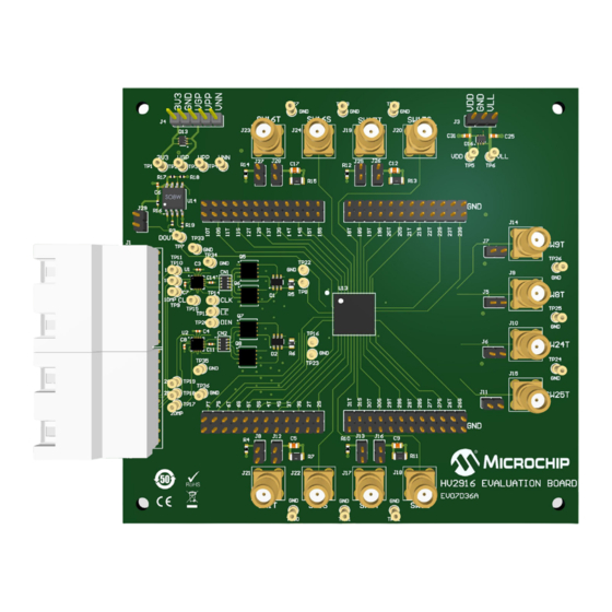
11. Clear the STBY check box and select the MODE check box. (Do not change these states. Not used for the HV2916 Analog Switch Evaluation Board.) 12. Click the Set HV MUX button. All digital control signals are applied to the HV2916 device. - Page 18 HV2916 Analog Switch Evaluation Board User’s Guide FIGURE 2-7: HV2916 ANALOG SWITCH EVALUATION BOARD FRONT VIEW 2.3.1 Recommended Power-Up and Power-Down Sequences Table 2-2 shows the recommended power-up and power-down sequences of the HV2916 Analog Switch Evaluation Board. TABLE 2-2:...
-
Page 19: Interface Connections
LVCMOS-2.5V Output EEPROM Serial Data Output J2-B3 MOSI — LVCMOS-2.5V Input EEPROM Serial Data input J2-A5 TP15 LVCMOS-3.3V Input HV2916 Latch Clear Logic Input J2-B5 TP14 LVCMOS-3.3V Input HV2916 Clock Logic Input J2-C5 TP12 LVCMOS-3.3V Input HV2916 Latch Enable Logic Input... -
Page 20: Hv Mux Controller Board Setup Procedure
PWR_OK(LD4) on the HV MUX Controller Board should light up green. A “Connected” message is displayed on the bottom left of the Status bar of the GUI. The HV MUX Controller Board is now ready to control the HV2916 Analog Switch Evaluation Board. -
Page 21: Testing The Hv2916 Analog Switch Evaluation Board
2. Start the GUI program. If the board is not connected, a “Not Connected” message is displayed in the Status bar located at the bottom left of the screen. 3. Power up the HV MUX Controller Board and HV2916 Analog Switch Evaluation Board as described in the previous sections. The prompt “Connected”, is displayed in the Status bar. - Page 22 HV2916 Analog Switch Evaluation Board User’s Guide The Ch1 and Ch2 of the oscilloscope in Figure 2-9 show the SW8T and the SW9T. FIGURE 2-9: TYPICAL WAVEFORM OF 2:1 MUX CONNECTED TO PULSER 50V/div 50V/div 2021 Microchip Technology Inc.
-
Page 23: Chapter 3. Gui Description
HV2916 device and built-in pulsers immediately. By clicking the Set HV MUX, Start and Stop buttons, and the control data set by the user in the GUI change operation of the HV2916 device and turns on/off the built-in pulsers in the HV2916 Analog Switch Evaluation Board. - Page 24 When this check box is selected, the CLR logic input is set to high and all the switches of the HV2916 device are set to off. When cleared, the CLR logic input is set to low and the 32 switches of HV2916 are set to ON/OFF states according to the DIN data entry.
-
Page 25: Chapter 4. Pcb Design And Layout Notes
Chapter 4. PCB Design and Layout Notes PCB LAYOUT TECHNIQUES FOR HV2916 The HV2916 Analog Switch Evaluation Board has an analog switch to pass high- voltage, high-current and high-frequency pulses. Good PCB design and layout are important to ensure the success of the implementation. - Page 26 HV2916 Analog Switch Evaluation Board User’s Guide NOTES: 2021 Microchip Technology Inc. DS50003160A-page 26...
-
Page 27: Appendix A. Schematics And Layouts
EVALUATION BOARD USER’S GUIDE Appendix A. Schematics and Layouts INTRODUCTION This appendix contains the following schematics and layouts for the HV2916 Analog Switch Evaluation Board (EV07D36A) and the HV MUX Controller Board (ADM00825). 1. HV2916 Analog Switch Evaluation Board (EV07D36A): •... -
Page 28: Ev07D36A - Schematic
1_DMP 1812 SW12S SW12T 100V TC6320 0612 OUTD SW13S SW13T SW13S SW13T SW14S SW14T SW14S SW14T SW15S SW15T SW15S SW15T HV2916 SW16S SW16T SW16S SW16T MD1822 2.55k TC6320 330pF 2512 SW17S SW17T SW17S SW17T 250V 0805 SW18S SW18T SW18S SW18T... -
Page 29: Ev07D36A - Top Silk
Schematics and Layouts EV07D36A – TOP SILK EV07D36A – TOP COPPER AND SILK 2021 Microchip Technology Inc. DS50003160A-page 29... -
Page 30: Ev07D36A - Top Copper
HV2916 Analog Switch Evaluation Board User’s Guide EV07D36A – TOP COPPER EV07D36A – INNER 1 AND 4 2021 Microchip Technology Inc. DS50003160A-page 30... -
Page 31: Ev07D36A - Inner 2
Schematics and Layouts EV07D36A – INNER 2 EV07D36A – INNER 3 2021 Microchip Technology Inc. DS50003160A-page 31... -
Page 32: Ev07D36A - Bottom Copper
HV2916 Analog Switch Evaluation Board User’s Guide EV07D36A – BOTTOM COPPER A.10 EV07D36A – BOTTOM COPPER AND SILK 2021 Microchip Technology Inc. DS50003160A-page 32... -
Page 33: Ev07D36A - Bottom Silk
Schematics and Layouts A.11 EV07D36A – BOTTOM SILK 2021 Microchip Technology Inc. DS50003160A-page 33... -
Page 34: Adm00825 - Schematic (Connection)
A.12 ADM00825 – SCHEMATIC (CONNECTION) FPGA01.SchDoc Connector.SchDoc MUPB001_PWR.SchDoc IO_2V5_0_P USB_TO_SPI.SchDoc IO_2V5_0_P IO_2V5_0_P IO_2V5_0_N SPI_CSBAR IO_2V5_0_N IO_2V5_0_N IO_2V5_1_P CSBAR CSBAR SPI_SCK IO_2V5_1_P IO_2V5_1_P IO_2V5_1_N SPI_MOSI IO_2V5_1_N IO_2V5_1_N MOSI MOSI SPI_MISO IO_2V5_2_P MISO MISO IO_2V5_2_P IO_2V5_2_P IO_2V5_2_N FPGA_RST IO_2V5_2_N IO_2V5_2_N IO_2V5_3_P FPGA_RST FPGA_RST SPI_RST IO_2V5_3_P... -
Page 35: Adm00825 - Schematic (Power Supply)
A.13 ADM00825 – SCHEMATIC (POWER SUPPLY) 22000 pF 0603 ON-POWER ON XAL6060 Via_2.5x1.5 20BQ030P 0.1 µF 10 µF 10 µF 10 µF 10 µF POWER 2.5 mm 10 µF 10 µF 10 µF 0603 0.1 µF 0603 0603 0805 0805 0805 0805 1206... -
Page 36: Adm00825 - Schematic (Usb To Spi)
A.14 ADM00825 – SCHEMATIC (USB TO SPI) 3V3_VDD C103 C106 4.7 µF 0.1 µF USB_CONFIG LED, ON- SUSPEND, OFF - ACTIVE 1206 0603 GND_D 0603 GND_D MCP2210 SSOP-20 12 MHz USB_D+ OSC1 OSC1 OSC1 USB MINI-B Female 3V3_VDD USB_D- OSC2 OSC2 OSC2 USB_D-... -
Page 37: Adm00825 - Schematic (Programmable Clock)
A.15 ADM00825 – SCHEMATIC (PROGRAMMABLE CLOCK) GND_D 0603 XTAL-40 MHz 0.1 µF 40MHz_N 100R GND_D 0603 40MHz_P 0.1 µF 0603 CLK5 3V3_CLK 100k GND_D GND_D C107 0603 4.7 µF 10000 pF 4.7 µF 0.010 µF 4700 pF 10000 pF 10000 pF 10000 pF 10000 pF 10000 pF... -
Page 38: Adm00825 - Schematic (Fpga)
A.16 ADM00825 – SCHEMATIC (FPGA) 3V3_VDD 4.7k 0603 OUT1 IO_L65N_CSO_B_2 EXT_INT IO_L66N_SCP0_0 CTRL_OEB IO_L83N_VREF_3 IO_2V5_0_N IO_L74N_DOUT_BUSY_1 INIT_B OUT2 IO_L65P_INIT_B_2 IO_L66P_SCP1_0 CTRL_OED IO_L83P_3 IO_2V5_0_P IO_L74P_AWAKE_1 IO_L64N_D9_2 IO_L65N_SCP2_0 CTRL_OEC IO_L52N_3 IO_2V5_1_N IO_L47N_1 IO_2V5_13_N IO_L64P_D8_2 MOSI IO_L65P_SCP3_0 CTRL_SDI IO_L52P_3 IO_2V5_1_P IO_L47P_1 IO_2V5_13_P IO_L62N_D6_2 MISO IO_L64N_SCP4_0 CTRL_CSB... -
Page 39: Adm00825 - Schematic (Fpga Decoupling Capacitors)
A.17 ADM00825 – SCHEMATIC (FPGA DECOUPLING CAPACITORS) For 1V2_VCCINT 1V2_VCCINT 100 µF 47 nF 1000 pF 1000 pF 1000 pF 1000 pF 1000 pF 6.3V TANT-B 0603 0603 0603 0603 0603 0603 GND_D For VCCO_1 For VCCAUX For VCCO_0 2V5_VDD 3V3_VDD 3V3_VDD 33 µF... -
Page 40: Adm00825 - Schematic (Connectors)
A.18 ADM00825 – SCHEMATIC (CONNECTORS) PWR5V0 PWR5V0 33 µF 33 µF 0.1 µF 0.1 µF TANT-B TANT-B 0603 0603 GND_D GND_D IO_2V5_0_P IO_2V5_15_P IO_2V5_0_N IO_2V5_15_N IO_2V5_1_P IO_2V5_2_P IO_2V5_16_P IO_2V5_17_P IO_2V5_1_N IO_2V5_2_N IO_2V5_16_N IO_2V5_17_N IO_2V5_3_P IO_2V5_4_P IO_2V5_18_P IO_2V5_19_P IO_2V5_3_N IO_2V5_4_N IO_2V5_18_N IO_2V5_19_N IO_2V5_5_P IO_2V5_6_P... -
Page 41: A.19 Adm00825 - Top Silk
Schematics and Layouts A.19 ADM00825 – TOP SILK A.20 ADM00825 – TOP COPPER AND SILK 2021 Microchip Technology Inc. DS50003160A-page 41... -
Page 42: A.21 Adm00825 - Top Copper
HV2916 Analog Switch Evaluation Board User’s Guide A.21 ADM00825 – TOP COPPER A.22 ADM00825 – INNER 1 2021 Microchip Technology Inc. DS50003160A-page 42... -
Page 43: Adm00825 - Inner 2
Schematics and Layouts A.23 ADM00825 – INNER 2 A.24 ADM00825 – INNER 3 2021 Microchip Technology Inc. DS50003160A-page 43... -
Page 44: Adm00825 - Inner 4
HV2916 Analog Switch Evaluation Board User’s Guide A.25 ADM00825 – INNER 4 A.26 ADM00825 – BOTTOM COPPER 2021 Microchip Technology Inc. DS50003160A-page 44... -
Page 45: A.27 Adm00825 - Bottom Copper And Silk
Schematics and Layouts A.27 ADM00825 – BOTTOM COPPER AND SILK A.28 ADM00825 – BOTTOM SILK 2021 Microchip Technology Inc. DS50003160A-page 45... - Page 46 HV2916 Analog Switch Evaluation Board User’s Guide NOTES: 2021 Microchip Technology Inc. DS50003160A-page 46...
-
Page 47: Appendix B. Bill Of Materials (Bom)
HV2916 ANALOG SWITCH EVALUATION BOARD USER’S GUIDE Appendix B. Bill of Materials (BOM) HV2916 ANALOG SWITCH EVALUATION BOARD – BOM TABLE B-1: HV2916 ANALOG SWITCH EVALUATION BOARD – BILL OF MATERIALS Qty. Reference Description Manufacturer Part Number C1, C2, C19, C20, Capacitor, Ceramic, 1 µF, 250V, 20%,... - Page 48 HV2916 Analog Switch Evaluation Board User’s Guide TABLE B-1: HV2916 ANALOG SWITCH EVALUATION BOARD – BILL OF MATERIALS Qty. Reference Description Manufacturer Part Number J9, J10, J14, J15, Connector, RF, Coaxial, SMA, Adam Equipment RF2-04A-T-00-50-G J17, J18, J19, J20, Female, 2P, TH, Vertical J21, J22, J23, J24 Connector, Header-2.54, Male, 1x2,...
-
Page 49: Hv Mux Controller Board - Bom
Bill of Materials (BOM) TABLE B-1: HV2916 ANALOG SWITCH EVALUATION BOARD – BILL OF MATERIALS Qty. Reference Description Manufacturer Part Number Microchip Analog Switch, HV2916, Microchip HV2916/AJA HV, 100V, BGA-121 Technology Inc. Microchip Memory Serial Flash 16M Microchip SST26VF016B-104I/SM 104MHz SST26VF016B-104I/SM Technology Inc. - Page 50 HV2916 Analog Switch Evaluation Board User’s Guide TABLE B-2: HV MUX CONTROLLER BOARD – BILL OF MATERIALS (CONTINUED) Qty. Reference Description Manufacturer Part Number C67, C68, C81, Capacitor, Ceramic, 0.1 µF, Samsung CL10B104KO8NNNC C82, C92, C93, 16V, 10%, X7R, Surface Mount,...
- Page 51 Panasonic - ECG ERJ-3EKF7502V 1%, 1/10W, Surface Mount, 0603 Note: The components listed in this Bill of Materials are representative of the PCB assembly. The released BOM used in manufacturing uses all RoHS-compliant components. 2021 Microchip Technology Inc. DS50003160A-page 51...
- Page 52 HV2916 Analog Switch Evaluation Board User’s Guide TABLE B-2: HV MUX CONTROLLER BOARD – BILL OF MATERIALS (CONTINUED) Qty. Reference Description Manufacturer Part Number R43,R45,R47 Resistor, Thick Film, 100 k, Panasonic - ECG — 1%, 1/10W, Surface Mount, 0603 R44, R46, R48 Resistor, 78.7 k...
-
Page 53: Appendix C. Demo Board Waveforms
SW8T (SW8 ON) 5V/div SW9T (SW9 OFF) 100V/div SW24T (SW24 ON) 5V/div SW25T (SW25 OFF) FIGURE C-2: 5 MHz, 10 Pulses, V = ±100V, V = +5V, VGP = 10V, 330 pF//2.5 kΩ Load. 2021 Microchip Technology Inc. DS50003160A-page 53... -
Page 54: Worldwide Sales And Service
New York, NY Tel: 46-31-704-60-40 Tel: 631-435-6000 Sweden - Stockholm San Jose, CA Tel: 46-8-5090-4654 Tel: 408-735-9110 UK - Wokingham Tel: 408-436-4270 Tel: 44-118-921-5800 Canada - Toronto Fax: 44-118-921-5820 Tel: 905-695-1980 Fax: 905-695-2078 2021 Microchip Technology Inc. DS50003160A-page 54 02/28/20...
Need help?
Do you have a question about the HV2916 and is the answer not in the manual?
Questions and answers