
Subscribe to Our Youtube Channel
Related Manuals for National Instruments GPIB-SBX


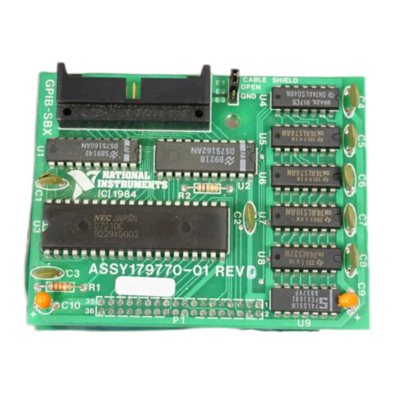
Summary of Contents for National Instruments GPIB-SBX
- Page 1 GPIB-SBX User Manual January 1996 Edition Part Number 320015-01 © Copyright 1983, 1996 National Instruments Corporation. All Rights Reserved.
- Page 2 National Instruments Corporate Headquarters 6504 Bridge Point Parkway Austin, TX 78730-5039 (512) 794-0100 Technical support fax: (800) 328-2203 (512) 794-5678 Branch Offices: Australia 03 9 879 9422, Austria 0662 45 79 90 0, Belgium 02 757 00 20, Canada (Ontario) 519 622 9310, Canada (Québec) 514 694 8521, Denmark 45 76 26 00, Finland 90 527 2321, France 1 48 14 24 24,...
- Page 3 Limited Warranty The GPIB-SBX is warranted against defects in materials and workmanship for a period of two years from the date of shipment, as evidenced by receipts or other documentation. National Instruments will, at its option, repair or replace equipment that proves to be defective during the warranty period. This warranty includes parts and labor.
- Page 4 Organization of the GPIB-SBX User Manual The GPIB-SBX User Manual is organized as follows: • Chapter 1, Introduction, contains a brief description of the GPIB-SBX kit, a list of equipment supplied, and a list of optional equipment. • Chapter 2, General Description, contains the physical and electrical specifications for the GPIB-SBX and describes the characteristics of key interface board components.
- Page 5 < less than ampere hexadecimal inch kbytes/sec 1,000 bytes per second 1,024 bytes of memory meter µA microampere µsec microsecond milliampere megahertz nsec nanosecond volt volts direct current GPIB-SBX User Manual © National Instruments Corporation...
- Page 6 If you encounter any technical problems, you can use the following toll-free number between the hours of 8:00 a.m. and 5:30 p.m. (central time) to reach the National Instruments applications engineering department: (512) 794-0100 (800) IEEE-488 (toll-free U.S.
-
Page 7: Table Of Contents
Contents Chapter 1 Introduction ......................... 1-1 GPIB-SBX Interface Kit Description ................1-1 What Your Kit Should Contain ..................1-2 Optional Equipment ...................... 1-2 Chapter 2 General Description ......................2-1 GPIB-SBX Specifications....................2-1 Physical Specifications ..................2-1 Electrical Specifications..................2-1 SBX Interface Bus Signals..................... 2-3 Control Lines...................... - Page 8 Going from Active to Standby Controller............5-3 Going from Standby to Active Controller............5-4 Going from Active to Idle Controller ..............5-4 The GPIB-SBX as GPIB Talker and Listener ............... 5-5 Programmed Implementation of Talker and Listener........5-5 Addressed Implementation of Talker and Listener..........5-5 Address Mode 1 ..................
- Page 9 GPIB Talker/Listener/Controller (TLC) ................ 6-2 GPIB Interface ....................... 6-3 Chapter 7 Diagnostic and Troubleshooting Test Procedures ..........7-1 Interpreting Test Procedures ..................7-1 GPIB-SBX Hardware Installation Tests ................ 7-2 Appendix A Parts List and Schematic Diagram ................A-1 Appendix B Sample Programs ........................
- Page 10 Contents Figures Figure 1-1. GPIB-SBX Interface Board ................1-1 Figure 2-1. GPIB-SBX with a Multibus Computer ............2-11 Figure 2-2. GPIB-SBX in a Multiprocessor Application............ 2-12 Figure 2-3. GPIB-SBX Block Diagram ................2-13 Figure 3-1. GPIB Cable Shield Grounding................. 3-1 Figure 3-2.
-
Page 12: Introduction
Introduction Chapter 1 What Your Kit Should Contain Your kit should contain the following components: Component Part Number GPIB-SBX Interface Board 179770-01 20-in. Interface Cable (chassis mount) 179753-01 GPIB-SBX User Manual 320015-01 Make sure each of these items is in your kit. If any item is missing, contact National Instruments. -
Page 13: General Description
The physical and electrical specifications are described in the following sections. Physical Specifications The GPIB-SBX measures 2.85 in. by 3.7 in. and is supplied with a 36-pin plug and spacing studs for mounting on the host board. A 26-pin male header connects to the GPIB adapter cable. -
Page 14: Table 2-2. Loading On Incoming Sbx Signal Lines
8 mA @ 0.35 V, -0.4 mA @ 3.4 V Additional circuitry permits the GPIB-SBX to automatically become System Controller or give up control automatically when the GPIB-SBX receives the Take Control or Release Control auxiliary commands. No special software support or hardware setting are necessary to make the GPIB-SBX System Controller or not System Controller. -
Page 15: Sbx Interface Bus Signals
• 2 Power Lines The following paragraphs describe the signals used by the GPIB-SBX. The GPIB-SBX uses 29 of the available 36 SBX bus signals. Table 2-4 lists all 36 signals and indicates which ones are used and which ones are not used. - Page 16 General Description Chapter 2 Table 2-4. GPIB-SBX Connector Pin Assignments (continued) Used/ Mnemonic Description Not Used MINTR0 M Interrupt 0 Used IORD* I/O Read Command Used MWAIT* M Wait Used Signal Ground Used +5 Volts Used M Data Bit 7...
-
Page 17: Control Lines
DMA cycle. TDMA is tied to ground so that it does not float to a true state. Initialize Line (MRESET) MRESET is an active-high signal used by the host board to place the GPIB-SBX in a known quiescent state. Clock Line (MCLK) MCLK is a 10-MHz timing signal provided by the host board to the GPIB-SBX. -
Page 18: Data Lines (Md7-Md0)
SBX bus. MD7 is the most significant bit. Interrupt Line (MINTR1-MINTR0) MINTR0 is an active-high signal generated by the GPIB-SBX to send an interrupt to the host board. MINTR1 is tied to ground so that it does not float to a true state. -
Page 19: Data Transfer Modes And Performance
In DMA mode, data is transferred directly between memory and the CDOR/DIR, using the facilities of a DMA Controller that is external to the GPIB-SBX (that is, it is a function of the host board or the computer system). The data transfer in this mode can exceed 500 kbytes/sec provided that the Controller, memory, and external GPIB devices are capable of sustaining this rate. -
Page 20: Gpib Signal Lines
16 signal lines are used to carry all information, interface messages, and device-dependent messages among interconnected devices. The 16 signal lines are organized into three sets, as follows: • 8 data input/output lines • 3 handshake lines • 5 interface management signal lines GPIB-SBX User Manual © National Instruments Corporation... - Page 21 Instruments that use the REN line must monitor it at all times and return to local control whenever it becomes false. The SRQ (Service Request) line is used by an instrument to asynchronously request service from the Controller-In-Charge. © National Instruments Corporation GPIB-SBX User Manual...
-
Page 22: Gpib Physical Characteristics
GPIB terminology, the GPIB-SBX implements GPIB interface functions for communicating with other GPIB devices and device functions for communicating with the central processor and memory. From the point of view of the host board, the GPIB-SBX is an interface to the outside world. -
Page 23: Figure 2-1. Gpib-Sbx With A Multibus Computer
NRFD (Not Ready for Data) NDAC (Not Data Accepted) Management Lines IFC (Interface Clear) 5 Lines ATN (Attention) SRQ (Service Request) REN (Remote Enable) EOI (End or Identity) Figure 2-1. GPIB-SBX with a Multibus Computer © National Instruments Corporation 2-11 GPIB-SBX User Manual... -
Page 24: Figure 2-2. Gpib-Sbx In A Multiprocessor Application
General Description Chapter 2 Figure 2-2 shows the GPIB-SBX used along with other National Instruments interface boards to connect a Multibus computer to other processors in order, for example, to transfer files electrically rather than manually (via a removable storage medium) or to perform other interprocessor communication functions. -
Page 25: Figure 2-3. Gpib-Sbx Block Diagram
Chapter 2 General Description Figure 2-3 is a block diagram of the GPIB-SBX-1. Data Transceiver Control Transceiver System Controller GPIB Adapter Select Figure 2-3. GPIB-SBX Block Diagram The interface consists of these major sections that are discussed in greater detail in Chapters 4, 5, and 6: •... -
Page 26: Table 2-6. Gpib-Sbx Ieee-488 Interface Capabilities
Special transceivers interface the TLC to the GPIB itself. Table 2-6 lists the capabilities of the GPIB-SBX in terms of the codes in Appendix C of the IEEE-488 standard. - Page 27 The GPIB-SBX has complete Source and Acceptor Handshake capability. • The GPIB-SBX can operate as a basic Talker or Extended Talker and can respond to a Serial Poll. It can be placed in a Talk Only mode, and is unaddressed to Talk when it receives its Listen address.
- Page 28 Initialize the interface • Send Remote Enable • Respond to Service Request • Send multiline command messages • Receive control • Pass control • Conduct a Parallel Poll • Take control synchronously or asynchronously GPIB-SBX User Manual 2-16 © National Instruments Corporation...
-
Page 29: Configuration And Installation
To GPIB-SBX Figure 3-1. GPIB Cable Shield Grounding Installation The GPIB-SBX is installed on a host board by means of the SBX connector and a nylon spacer provided in the interface kit. Warning: Never attempt to install the GPIB-SBX on a host board that has power applied to it. -
Page 30: Figure 3-2. Gpib-Sbx Installed On Host Board
2. Place the nylon threaded spacer between the component side of the host board and the circuit side of the GPIB-SBX directly in line with the mounting holes provided. 3. Insert screws from the component side of the GPIB-SBX into the spacer and from the circuit side of the host board into the spacer. -
Page 31: Cabling
GPIB device. The cable is generally run through the back panel of the computer and strain relieved in some manner. Both cables connect to the GPIB-SBX at the right-angle header labeled J1 at the top of the circuit card. Take care when installing the connector. Pin 26 of the cable connector and the associated pin of the J1 are keyed to prevent the connectors from being installed backwards. -
Page 32: Verification Testing
Figure 3-4. GPIB-SBX Cable-to-Interface Board Connection Verification Testing The GPIB-SBX is tested twice and receives a 96-hour burn-in before shipment. Nonetheless, a performance verification test should be run to ensure that the board has not been damaged during shipment and also to ensure that the board has been configured correctly. To do this requires an interactive control program or an equivalent mechanism, such as front panel control switches or front panel emulator, that can load and read memory and I/O addresses. -
Page 33: Register Descriptions
Register Descriptions Introduction All software control of the GPIB-SBX is performed through a set of interface registers located within a block of eight consecutive I/O addresses. Some of the registers are read only and some are write only. Some registers are not storage registers at all, but buffers through which status signals can be read or through which control pulses can be sent. -
Page 34: Interface Registers
(MA2-MA0), the I/O Read or Write command (IORD, IOWRT*), and the SBX device select command. Figures 4-1 and 4-2 show the register and bit mnemonics of each GPIB-SBX register, its I/O port offset, and its read/write accessibility (the value of MA2-MA0). Figure 4-1 shows the regular GPIB-SBX interface registers. -
Page 35: Figure 4-1. Gpib-Sbx Interface Registers
AD5-0 AD4-0 AD3-0 AD2-0 AD1-0 ADR0 ADR1 AD5-1 AD4-1 AD3-1 AD2-1 AD1-1 EOS7 EOS6 EOS5 EOS4 EOS3 EOS2 EOS1 EOS0 EOSR Note: X indicates a don't care bit. Figure 4-1. GPIB-SBX Interface Registers © National Instruments Corporation GPIB-SBX User Manual... -
Page 36: Figure 4-2. Writing To The Hidden Registers
CLK1 CLK0 PPR is loaded with: AUXRA is loaded with: XEOS REOS HLDE HLDA AUXRB is loaded with: SPEOI ENABLE AUXRE is loaded with: DHDT DHDC Figure 4-2. Writing to the Hidden Registers GPIB-SBX User Manual © National Instruments Corporation... -
Page 37: Data In Register (Dir)
DI0 is the least significant bit of the data byte and corresponds to GPIB DI01. DI7 is the most significant bit of the data byte and corresponds to GPIB DI08. Mnemonic Description 7-0r DI[7-0] Data In Bits 7 through 0 © National Instruments Corporation GPIB-SBX User Manual... -
Page 38: Command/Data Out Register (Cdor)
DIR. When a byte is written to the CDOR, the TLC GPIB Source Handshake (SH) function is initiated and the byte is transferred to the GPIB. Mnemonic Description 7-0w CDO[7-0] Command/Data Out Bits 7 through 0 GPIB-SBX User Manual © National Instruments Corporation... -
Page 39: Interrupt Status Register 1 (Isr1)
-(CPT ENABLE) + UDPCF & SCG & ACDS & CPT ENABLE CPT is cleared by: pon + (read ISR1) Notes UCG: GPIB Universal Command Group message ACG: GPIB Addressed Command Group message TADS: GPIB Talker Addressed State LADS: GPIB Listener Addressed State © National Instruments Corporation GPIB-SBX User Manual... - Page 40 Address Pass Through APT IE Address Pass Through Interrupt Enable APT is set by: ADM1 & ADM0 & (TPAS + LPAS) & SCG & ACDS APT is cleared by: pon + (read ISR1) GPIB-SBX User Manual © National Instruments Corporation...
- Page 41 Listener (the TLC has been in DTAS). END RX End Received Bit END IE End Received Interrupt Enable Bit END RX is set by: LACS & (EOI + EOS & REOS) & ACDS © National Instruments Corporation GPIB-SBX User Manual...
- Page 42 Error Interrupt Enable Bit ERR is set by: TACS & SDYS & DAC & RFD + SIDS & (write CDOR) + (SDYS to SIDS) ERR is cleared by: pon + (read ISR1) GPIB-SBX User Manual 4-10 © National Instruments Corporation...
- Page 43 SBX bus for transmission onto the GPIB when the TLC is the GPIB Talker. The DO bit is cleared when a byte is written to the CDOR and also when the TLC ceases to be the Active Talker. © National Instruments Corporation 4-11 GPIB-SBX User Manual...
- Page 44 Finish Handshake auxiliary command issued Holdoff mode: RFD Holdoff state read DIR: Read Data In Register The DI bit indicates that the TLC, as a GPIB Listener, has accepted a data byte from the GPIB Talker. GPIB-SBX User Manual 4-12 © National Instruments Corporation...
-
Page 45: Interrupt Status Register 2 (Isr2)
DEC IE) + (DO & DO IE) + (DI & DI IE) + (SRQI & SRQI IE) + (REMC & REMC IE) + (CO & CO IE) + (LOKC & LOKC IE) + (ADSC & ADSC IE) Unused Bit Write zero to this bit. © National Instruments Corporation 4-13 GPIB-SBX User Manual... - Page 46 (RWLS). The TLC RL function transfers to one of these states when the System Controller has asserted the Remote Enable line (REN), and the CIC addresses the TLC as a Listener. DMAI DMA Input Enable Bit GPIB-SBX User Manual 4-14 © National Instruments Corporation...
- Page 47 LOKC is set when there is a change in the LOK bit, ISR2[5]r, (REMS + RWLS). REMC Remote Change Bit REMC IE Remote Change Interrupt Enable Bit REMC is set by: any change in REM REMC is cleared by: pon + (read ISR2) © National Instruments Corporation 4-15 GPIB-SBX User Manual...
- Page 48 ADSR: Address Status Register ADMR: Address Mode Register ADSC is set when there is a change in one of the four bits TA, LA, CIC, MJMN of the Address Status Register (ADSR). GPIB-SBX User Manual 4-16 © National Instruments Corporation...
-
Page 49: Serial Poll Status Register (Spsr)
STB during the poll, the TLC clears rsv at the Affirmative Poll Response State (APRS). The rsv bit is also cleared by pon, and by issuing the Chip Reset auxiliary command. © National Instruments Corporation 4-17 GPIB-SBX User Manual... -
Page 50: Address Status Register (Adsr)
Address Mode Register in this chapter), LPAS=1 indicates that the secondary address being received on the next GPIB command may represent the TLC extended (secondary) GPIB listen address. LPAS is cleared by pon, or by issuing the Chip Reset auxiliary command. GPIB-SBX User Manual 4-18 © National Instruments Corporation... - Page 51 (mode 1 or mode 3) is enabled (see Address Mode Register in this chapter). The MJMN bit is cleared by pon or by issuing the Chip Reset auxiliary command. © National Instruments Corporation 4-19 GPIB-SBX User Manual...
-
Page 52: Address Mode Register (Admr)
TRM[1-0] Transmit/Receive Mode Bit TRM1 and TRM0 control the function of the TLC T/R2 and T/R3 output pins in the following manner: TRM1 TRM0 T/R2 T/R3 EOI OE TRIG TRIG EOI OE GPIB-SBX User Manual 4-20 © National Instruments Corporation... - Page 53 2 addressing implements the Extended Talker and Extended Listener functions as defined in IEEE-488, without requiring computer program intervention. In mode 2, ADR0 and ADR1 contain the TLC primary and secondary GPIB addresses, respectively. © National Instruments Corporation 4-21 GPIB-SBX User Manual...
- Page 54 Acceptor Handshake is held up in the Accept Data State (ACDS) until the Valid or Non-Valid auxiliary command is written to the AUXMR, signaling a valid or invalid secondary address, respectively, to the TLC. GPIB-SBX User Manual 4-22 © National Instruments Corporation...
-
Page 55: Command Pass Through Register (Cptr)
Parallel Poll response. The PPR message is latched into the CPTR when CPPS is set, and held valid until CIDS is set, or until a command byte is sent over the GPIB. © National Instruments Corporation 4-23 GPIB-SBX User Manual... -
Page 56: Auxiliary Mode Register (Auxmr)
Table 4-3 explains the details of each special function. If the control code is not 000, these bits are written to one of the hidden registers (indicated by the control code in CNT[2-0]). GPIB-SBX User Manual 4-24 © National Instruments Corporation... -
Page 57: Table 4-2. Auxiliary Command Summary
Set REN 1 0 1 1 1 Clear REN 1 0 1 0 0 Disable System Control * CNT[2-0] set to 000 binary ** Represents all eight bits of the Auxiliary Mode Register © National Instruments Corporation 4-25 GPIB-SBX User Manual... -
Page 58: Table 4-3. Auxiliary Commands: Detail Description
The TRM0 bit and the TRM1 bit are cleared. Once a Chip Reset command is executed, an Immediate Execute pon command must be executed before the TLC can be programmed or addressed. (continues) GPIB-SBX User Manual 4-26 © National Instruments Corporation... - Page 59 Holdoff on RFD or DAC. 0 0 1 0 0 Trigger Note: Trigger is not implemented on the GPIB-SBX. The Trigger command generates a high pulse on the TRIG pin (T/R3 pin when TRM1=0) of the TLC. The Trigger command performs the same function as if the DET (Device Trigger) bit (ISR1[5]r) were set.
- Page 60 TLC enters CACS. 1 0 0 1 1 Listen The listen command generates the local message ltn in the form of a pulse. It should be issued when the controller is in CACS. (continues) GPIB-SBX User Manual 4-28 © National Instruments Corporation...
- Page 61 Control (rsc) and set Interface Clear (IFC) to the value of COM3. In order to meet IEEE-488 requirements, you must not issue the Clear IFC command until IFC has been held true for at least 100 µsec. (continues) © National Instruments Corporation 4-29 GPIB-SBX User Manual...
- Page 62 Set REN command until REN has been held false for at least 100 µsec. 1 0 1 0 0 Disable System Control The Disable System Control command clears the local message rsc. GPIB-SBX User Manual 4-30 © National Instruments Corporation...
-
Page 63: Hidden Registers
AUXRB bit TRI. For proper operation in the GPIB-SBX, ICR should be set to five because the TLC is clocked at 5 MHz. © National Instruments Corporation... -
Page 64: Parallel Poll Register (Ppr)
(to the PPR) is the same as the receipt of the PPE message from the GPIB Controller. When U=1, S and P[3-1] do not carry any meaning, but they should be cleared. GPIB-SBX User Manual 4-32 © National Instruments Corporation... -
Page 65: Table 4-4. Examples For Configuring The Ppr
0 1 1 1 0 0 0 0 Unconfigures PPR 0 1 1 0 0 0 0 0 0 0 0 0 0 is written to the PPR. The GPIB-SBX participates in a Parallel Poll, asserting the DIO1 line if ist=0. Otherwise, the GPIB-SBX does not participate. -
Page 66: Auxiliary Register A (Auxra)
EOS message when the TLC is in Listener Active State (LACS). If REOS is set and the byte in the DIR matches the byte in the EOSR, the END RX bit (ISR1[4]r) is set. GPIB-SBX User Manual 4-34 © National Instruments Corporation... - Page 67 (no data reception). In continuous mode, the DI bit (ISR1[0]r) is not set by the reception of a data byte. © National Instruments Corporation 4-35 GPIB-SBX User Manual...
-
Page 68: Auxiliary Register B (Auxrb)
The INV bit affects the polarity of the TLC INT pin. Setting INV causes the polarity of the Interrupt (INT) pin on the TLC to be active low. As implemented on the GPIB-SBX, configuring the INT pin to active low results in interrupt request errors. - Page 69 The TRI bit determines the TLC GPIB Source Handshake Timing, T1. TRI can be set to enable high-speed data transfers (T1 ≥ 500 nsec) when tri-state GPIB drivers are used. (The GPIB-SBX uses tri-state GPIB drivers except during Parallel Poll responses, in which case the GPIB drivers automatically switch to Open Collector.) Setting TRI enables high-speed timing as T1 of the...
-
Page 70: Auxiliary Register E (Auxre)
DAC Holdoff on DCAS Bit Setting DHDC enables DAC Holdoff when the TLC enters Device Clear Active State (DCAS). Clearing DHDC disables DAC Holdoff on DCAS. Issuing the Finish Handshake auxiliary command releases the Holdoff. GPIB-SBX User Manual 4-38 © National Instruments Corporation... -
Page 71: Address Register 0 (Adr0)
These are the lower 5 bits of the TLC GPIB primary (or major) address. The primary talk address is formed by adding hex 40 to AD[5-0—1-0], while the listen address is formed by adding hex © National Instruments Corporation 4-39 GPIB-SBX User Manual... -
Page 72: Address Register (Adr)
GPIB listen address is formed by adding hex 20. The value written to AD[5-1] should not be all ones, since the corresponding talk and listen addresses would conflict with the GPIB Untalk (UNT) and GPIB Unlisten (UNL) commands. GPIB-SBX User Manual 4-40 © National Instruments Corporation... -
Page 73: Address Register 1 (Adr1)
(or minor primary listen address) formed from bits AD[5-1—1-1]. If DL1 is cleared and the TLC received its primary listen address (that is, is in LPAS), the secondary address is checked. © National Instruments Corporation 4-41 GPIB-SBX User Manual... - Page 74 The secondary address is formed by adding hex 60 to bits AD[5-1—1-1]. The minor talk address is formed by adding hex 40 to AD[5-1—1-1], while the listen address is formed by adding a hex 20. GPIB-SBX User Manual 4-42 © National Instruments Corporation...
-
Page 75: End Of String Register (Eosr)
XEOS of AUXRA is set, the END message (GPIB EOI* line asserted low) is sent along with the data byte whenever the contents of the CDOR matches the EOSR. Mnemonic Description 7-0w EOS[7-0] End of String Bits 7 through 0 © National Instruments Corporation 4-43 GPIB-SBX User Manual... -
Page 76: Programming Considerations
A typical programming initialization sequence for the GPIB-SBX might include the following steps: 1. Write the Chip Reset command to the AUXMR to place the GPIB-SBX in a known quiescent state. 2. Set or clear the desired Interrupt Enable bits in the Interrupt Mask Register 1 (IMR1) and the Interrupt Mask Register 2 (IMR2). -
Page 77: The Gpib-Sbx As Gpib Controller
8. Execute the desired auxiliary commands. The GPIB-SBX as GPIB Controller The GPIB-SBX Controller function is generally in one of two modes: idle or in charge. When in charge, the Controller function is either active (asserting Attention (ATN)) or standby (not asserting ATN). -
Page 78: Sending Remote Multiline Messages (Commands)
Control/Data Out Register (CDOR) in response to the CO status bit in ISR2. The GPIB-SBX can address itself to be both Talker and Listener in address mode 1 or 2; that is, the TLC recognizes its address when it sends or receives it. -
Page 79: Going From Standby To Active Controller
Status Register 1 (ISR1). This indicates that a Holdoff is in progress. When the tcs auxiliary command is used, the GPIB-SBX takes control of the GPIB only at the end of a data transfer. This implies that one transfer must follow or be in progress when the tcs auxiliary command is issued. -
Page 80: The Gpib-Sbx As Gpib Talker And Listener
Addressed Implementation of Talker and Listener When the GPIB-SBX is the GPIB Active Controller, it can address itself to talk or listen by sending its own GPIB talk or listen address using the CO bit and the CDOR. When there is another device on the GPIB acting as Controller, the GPIB-SBX is addressed with GPIB command messages to become a Talker or Listener. -
Page 81: Address Mode 2
Read the secondary address in the CPTR and determine whether or not it is the address of the GPIB-SBX. 5. If it is not the GPIB-SBX address, issue the Non-Valid auxiliary command. If it is the GPIB- SBX address, issue the Valid auxiliary command. -
Page 82: Sending/Receiving Messages
7. If the Non-Valid auxiliary command is issued, the GPIB-SBX assumes that an Other Secondary Address (OSA) message has been received, which causes: • The GPIB-SBX Talker or Listener function to go to its idle state (TIDS=1 or LIDS=1) if either the TPAS or LPAS bit was set; and •... -
Page 83: Sending And Receiving Data (Dma Mode)
Programming Considerations Chapter 5 To receive data, wait until the GPIB-SBX has been programmed or addressed to listen and the CDOR is empty. When this occurs, the DI bit in the ISR1 is set, indicating that the GPIB Talker has written a byte to the DIR. Once that byte has been read, the DI bit is set again when a new byte is received from the GPIB Talker. -
Page 84: Conducting Serial Polls
Before requesting service, you must check the Pending (PEND) bit of the SPSR to ensure that the GPIB-SBX is not presently in the middle of a Serial Poll (SPAS=0). If PEND=0, write the desired Status Byte (STB) to the SPMR with the rsv bit set. At that time, PEND sets and remains set until the Serial Poll (SP) completes. -
Page 85: Conducting A Parallel Poll
Parallel Poll auxiliary command is issued and the GPIB-SBX internal local message rpp is set, the PP is executed (that is, the GPIB message IDY is sent true) as soon as the GPIB-SBX Controller interface function is placed in the proper state (CAWS or CACS). The PPR is automatically read from the GPIB DIO line into the CPTR and the rpp local message is cleared. -
Page 86: Responding To A Parallel Poll
AUXRB is zero, ist is set and cleared via the Set and Clear Parallel Poll auxiliary commands. If ISS is one, ist is set if the Service Request function of the GPIB-SBX is in the Service Request State (SRQS) and the GPIB-SBX is asserting the GPIB SRQ signal line and cleared otherwise. -
Page 87: Chapter 6 Theory Of Operation
• DMA acknowledge extender The TLC, which is the heart of the GPIB-SBX, is discussed in greater detail in the GPIB Interface section later in this chapter. The System Controller (SC) selection circuit decodes auxiliary commands written to the TLC and sets or clears the SC flip-flop when specified commands are detected. -
Page 88: Gpib Talker/Listener/Controller (Tlc)
The Internal Clock Register (ICR) is used to set critical timing parameters based on the frequency of the TLC input clock, which on the GPIB-SBX is 5 MHz. The Parallel Poll Register (PPR) is used to locally configure the TLC for polling. Auxiliary Registers A, B, and E GPIB-SBX User Manual ©... -
Page 89: Gpib Interface
ATN and SRQ signals. T/R3 is high when the three- state driver mode is active and low when the open collector mode is active; when the GPIB-SBX is parallel polled, the transceiver switches to open collector mode during the poll. SC is set as explained in the SBX Bus Interface section earlier in this chapter. -
Page 90: Diagnostic And Troubleshooting Test Procedures
For this reason, users are advised to perform the tests in the order given. If the GPIB-SBX does not perform as described in the test procedures, carefully perform the following steps. 1. Verify that the test instructions have been followed correctly. -
Page 91: Gpib-Sbx Hardware Installation Tests
Chapter 7 After these items have been carefully checked, if the interface is still not functioning properly, gather together the information concerning what the GPIB-SBX is and is not doing with regard to the expected results and contact National Instruments. - Page 92 Immediate execute pon AUXMR = 1E set IFC AUXMR = 16 clear IFC ADSR = 80? ISR2 = 9? CO + ADSC AUXMR = 10 go to standby ADSR = CO? CIC + ATN* © National Instruments Corporation GPIB-SBX User Manual...
-
Page 93: Parts List And Schematic Diagram
Appendix A Parts List and Schematic Diagram This appendix contains the parts list and schematic diagram for the GPIB-SBX. © National Instruments Corporation GPIB-SBX User Manual... -
Page 97: Appendix B Sample Programs
8088 code appears on the left, 8080 code appears in the middle, and comments applying to both sets of code are on the right. Assumptions regarding the state of the GPIB-SBX appear at the beginning of each routine and must be adhered to for proper, error-free operation. - Page 98 For example, a comment written as ; Status on exit: -The bx(bc) register pair contains . . . indicates that the 8088 code uses the bx register pair, while the 8080 code uses the bc register pair. GPIB-SBX User Manual © National Instruments Corporation...
- Page 99 Appendix B Sample Programs ;;;;;;;;;;;;;;;;;;;;;;;;;;;;;;;;;;;;;;;;;;;;; ; GPIB-SBX Sample Functions for Driver: ; INIT (Initialize the GPIB-SBX) ; IFC (Send Interface Clear) REN (Set/Clear Remote Enable) ; RCV (Receive) READ (Read Data) DSEND (Data Send) WRITE (Write Data) CSEND (Command Send)
- Page 100 NATN equ 100q ; Not ATN ; ADMR Bits MODE1 equ 001q ; Address Mode 1 060q ; GPIB-SBX functions for T/R2 and T/R3 ; AUXMR Hidden Registers 040q ; Internal Counter Register 140q ; Parallel Poll Register AUXRA equ 200q ;...
- Page 101 - The following registers are cleared: ISR1/2, IMR1/2, SPMR, SPSR, PPR, AUXRA, AUXRB, AUXRE - Other registers are configured as described - The GPIB-SBX interface functions are reset to their idle states and are enabled © National Instruments Corporation GPIB-SBX User Manual...
- Page 102 ; * * * * * * * * * * * * * * * ; Summary: - Initialize the interface function of other GPIB devices ; Assumptions on entry: - GPIB-SBX has been initialized ; Actions: - Assert GPIB IFC (the interface automatically becomes System Controller and Active Controller)
- Page 103 ; Assumptions on entry: - User specified sre is non-zero if REN is to be asserted and is zero if REN is to be unasserted - GPIB-SBX is System Controller and Active Controller ; Actions: - Check sre flag. if non-zero (true) send REN else send clear REN ;...
- Page 104 GPIB-SBX is Idle Controller ; Assumptions on entry: - GPIB-SBX is Standby or Idle Controller - GPIB-SBX is or will be addressed to listen - The GPIB Talker has been or will be addressed - The Talker will send END with last byte...
- Page 105 ; Yes--continue RCV6 ; RCV6 ; No--exit RCV5: ;RCV5: al,DIR ; ; END--read last byte byte ptr [di],al bx,cx ; ; Record bytes read RCV6: ;RCV6: al,AUXRA+1; AUXRA+1 ; Send HLDA AUXMR,al; AUXMR © National Instruments Corporation GPIB-SBX User Manual...
- Page 106 ; * READ * ; * * * * * * ; Summary: - Called to read device dependent (data) messages when the GPIB-SBX is Controller- In-Charge (RCV is called when the GPIB-SBX is Idle Controller) ; Assumptions on entry:...
- Page 107 CMD call CMD ; Command routine will address the Talker al,LTN ; a,LTN ; Program GPIB-SBX to be a Listener AUXMR,al; AUXMR ; so it can take control synchronously al,GTS ; a,GTS ; later; then go to standby and drop ATN AUXMR,al;...
- Page 108 - The GPIB-SBX is Standby or Idle Controller - GPIB-SBX is or will be addressed to talk - If the GPIB-SBX is Idle Controller, the current CIC will go to standby - The bx(bc) register pair contains the byte count...
- Page 109 AUXMR,al; AUXMR DSEND2: mov al,byte ptr [si] ; ;DSEND2:mov ; Next byte CDOR,al ; CDOR DSEND1 ; DSEND1 DSEND3: mov bx,177777q ;DSEND3:mvi b,377q ; Return (-1) indicating error c,377q DSEND4: ret ;DSEND4:ret © National Instruments Corporation B-13 GPIB-SBX User Manual...
- Page 110 ; Actions: - Set up cmdbuf and cmdct and call CMD to address the GPIB-SBX as Talker, to address the Listener, and to unaddress all other devices - Go to standby and unassert ATN - Transfer the contents of datct to the...
- Page 111 ; Wait until last byte has been sent al,DO ; WRITE1 ; WRITE1 al,TCA ; a,TCA ; Then take control AUXMR,al; AUXMR cmdct ; Prepare to unaddress all Talkers cmdct ; ; and Listeners cmdct call CMD call CMD © National Instruments Corporation B-15 GPIB-SBX User Manual...
- Page 112 ; Summary: - Called by CMD to send interface (command) messages ; Assumptions on entry: - The GPIB-SBX is Active Controller - The bl(b) register contains the number of bytes to send - The si(hl) register pair contains the address of cmdbuf ;...
- Page 113 ; Summary: - Send GPIB interface or command messages ; Assumptions on entry: - The GPIB-SBX is Controller-In-Charge - The commands to be sent are in cmdbuf - The variable cmdct contains the number of commands to be sent, which must be...
- Page 114 GPIB-SBX is at standby - Set up the command buffer and command count - Call CMD to send the command bytes ; Status on return: - The GPIB-SBX is Idle Controller ; 8088 Code 8080 Code Comments ;----------------------- ---------------------------- ; ------------------------------------------------ PASSC: mov al,TCA ;PASSC: mvi...
-
Page 115: Multiline Interface Messages
These multiline interface messages are sent and received with ATN TRUE. For more information on these messages, refer to the ANSI/IEEE Std 488.1-1987, IEEE Standard Digital Interface for Programmable Instrumentation. © National Instruments Corporation GPIB-SBX User Manual... - Page 116 MLA27 < MLA28 MLA29 > MLA30 Message Definitions Device Clear My Secondary Address Group Execute Trigger My Talk Address Go To Local Parallel Poll Configure Local Lockout Parallel Poll Disable My Listen Address GPIB-SBX User Manual © National Instruments Corporation...
- Page 117 MTA24 MSA24,PPD MTA25 MSA25,PPD MTA26 MSA26,PPD MTA27 MSA27,PPD MTA28 MSA28,PPD MTA29 MSA29,PPD MTA30 MSA30,PPD Parallel Poll Enable Serial Poll Enable Parallel Poll Unconfigure Take Control Selected Device Clear Unlisten Serial Poll Disable Untalk © National Instruments Corporation GPIB-SBX User Manual...
-
Page 118: Appendix D Mnemonics Key
SBX bus signals. The mnemonic types in the key that follows are abbreviated to mean the following: Function Integrated Circuit Local Message Register Remote Message State SBX Bus Signal © National Instruments Corporation GPIB-SBX User Manual... - Page 119 Control/Data Out Bits 7 through 0 Controller-In-Charge Bit CIDS Controller Idle State CLK[3-0] Clock Bits 3 through 0 CNT[2-0] Control Code Bits 2 through 0 Command Output Bit CO IE Enable Interrupt on Command Output Bit GPIB-SBX User Manual © National Instruments Corporation...
- Page 120 Direct Memory Access Input Enable Bit DMAO Direct Memory Access Output Enable Bit Data Out Bit DO IE Enable Interrupt on Data Out Bit Device Trigger Disable Talker Bit Disable Talker 0 Bit © National Instruments Corporation GPIB-SBX User Manual...
- Page 121 HLDA Holdoff on All Bit HLDE Holdoff on End Bit Internal Count Register Identify Interface Clear IMR1 Interrupt Mask Register 1 IMR2 Interrupt Mask Register 2 Interrupt Bit Invert Bit IORD* I/O Read GPIB-SBX User Manual © National Instruments Corporation...
- Page 122 Chip Select 1, Connector C MD[7-1] Data Lines MDACK* DMA Acknowledge MDRQT DMA Request MINTRA0 Interrupt 0, Connector A MINTRA1 Interrupt 1, Connector A MINTRB0 Interrupt 0, Connector B MINTRB1 Interrupt 1, Connector B © National Instruments Corporation GPIB-SBX User Manual...
- Page 123 Parallel Poll Configure Parallel Poll Disable Parallel Poll Enable PPIS Parallel Poll Idle State Parallel Poll Response Parallel Poll Register PPSS Parallel Poll Standby Active Parallel Poll Unconfigure PUCS Parallel Poll Unaddressed to Configure State GPIB-SBX User Manual © National Instruments Corporation...
- Page 124 Serial Poll Idle State SPMR Serial Poll Mode Register SPMS Serial Poll Mode State Bit SPMS Serial Poll Mode State SPSR Serial Poll Status Register Service Request SRAS System Control Remote Enable Active State © National Instruments Corporation GPIB-SBX User Manual...
- Page 125 Three-State Timing Bit TRM[1-0] Transmit/Receive Mode Bits 1 through 0 Unconfigure Bit Universal Command Group UDPCF Undefined Primary Command Unlisten command Untalk command Don't Care Bit XEOS Transmit End with End Of String Bit GPIB-SBX User Manual © National Instruments Corporation...
- Page 126 User Comment Form National Instruments encourages you to give us your comments on the documentation supplied with its products. This information helps us provide quality products to meet your needs. Title: GPIB-SBX User Manual Edition Date: January 1996 Part Number: 320015-01 Please comment on the completeness, clarity, and organization of the manual.
-
Page 127: Index
ATN line, 2-9 ATN signal, 2-7 auxiliary commands detailed description, 4-26 to 4-30 summary table, 4-25 Auxiliary Mode Register (AUXMR) command summary (table), 4-25 detailed description (table), 4-26 to 4-30 operation of, 6-2 © National Instruments Corporation Index-1 GPIB-SBX User Manual... - Page 128 Auxiliary Register E (AUXRE), 4-38, 6-2 BIN (Binary Bit), 4-34 bus signals. See signals and lines. cabling of GPIB-SBX, 3-3 capability codes for GPIB-SBX, 2-14 to 2-16 CDO[7-0] (Command/Data Out Bits 7 through 0), 4-6 CDOR. See Command/Data Out Register (CDOR). Chip Reset command...
- Page 129 See X (Don't Care Bit). DT (Disable Talker Bit), 4-40 DT0 (Disable Talker 0 Bit), 4-39 DT1 (Disable Talker 1 Bit), 4-41 © National Instruments Corporation Index-3 GPIB-SBX User Manual...
- Page 130 1-2 parts list and schematic diagrams, A-1 to A-5 physical characteristics, 2-9 signal lines, 2-8 to 2-9 GPIB TLC. See Talker/Listener/Controller (TLC). ground and power lines (+5 V, +-12 V, GND), 2-6 GPIB-SBX User Manual Index-4 © National Instruments Corporation...
- Page 131 Parallel Poll Register (PPR), 4-32 to 4-33 HLDA (Holdoff on All Bit), 4-35 HLDE (Holdoff on END Bit), 4-35 ICR. See Internal Counter Register (ICR). IEEE-488 interface capabilities of GPIB-SBX, 2-14 to 2-16 IFC (Interface Clear) line, 2-9 Immediate Execute Pon command codes for, 4-25 description, 4-26 IMR1.
- Page 132 IORD* command line, 2-5 IOWRT* command line, 2-5 ISR1. See Interrupt Status Register 1 (ISR1). ISR2. See Interrupt Status Register 2 (ISR2). jumpers for configuring GPIB-SBX, 3-1 LA (Listener Active Bit), 4-19 lines. See signals and lines. Listen command codes for, 4-25...
- Page 133 Non-Valid Secondary Command or Address command codes for, 4-25 description, 4-27 NRFD (Not Ready for Data) line, 2-8 optional equipment for GPIB-SBX, 1-2 P[3-1] (Parallel Poll Response Bits 3 through 1), 4-33 Parallel Poll Register (PPR), 4-32 to 4-33, 6-2 parallel polls...
- Page 134 5-9 to 5-11 sample programs COMMAND-CMD, B-19 COMMAND SEND-CSEND, B-18 DATA SEND-DSEND, B-14 to B-15 GPIB-SBX Sample Functions for Driver, B-3 to B-5 INITIALIZE-INIT, B-6 to B-7 INTERFACE CLEAR-IFC, B-8 overview, B-1 to B-2 READ, B-12 to B-13...
- Page 135 S8 (Serial Poll Status Bit 8), 4-17 sample programs COMMAND-CMD, B-19 COMMAND SEND-CSEND, B-18 DATA SEND-DSEND, B-14 to B-15 GPIB-SBX Sample Functions for Driver, B-3 to B-5 INITIALIZE-INIT, B-6 to B-7 INTERFACE CLEAR-IFC, B-8 overview, B-1 to B-2 READ, B-12 to B-13...
- Page 136 2-3 initialize line (MRESET), 2-5 internal registers (table), 2-6 interrupt line (MINTR1-MINTR0), 2-6 pin assignments (table), 2-3 to 2-4 power and ground lines (+5 V, +-12 V, GND), 2-6 GPIB-SBX User Manual Index-10 © National Instruments Corporation...
- Page 137 TDMA DMA line, 2-5 Technical support, vii terminology used in the manual, vi test and troubleshooting. See troubleshooting test procedures. theory of operation GPIB interface, 6-3 SBX bus interface, 6-1 Talker/Listener/Controller (TLC), 6-2 to 6-3 © National Instruments Corporation Index-11 GPIB-SBX User Manual...
- Page 138 TRM[1-0] (Transmit/Receive Mode Bits 1 through 0), 4-20 troubleshooting test procedures hardware installation tests, 7-2 to 7-3 interpreting test procedures, 7-1 overview, 7-1 verification of GPIB-SBX before installation, 3-4 U (Parallel Poll Unconfigure Bit), 4-32 Valid Secondary Command or Address command codes for, 4-25 description, 4-27...
Need help?
Do you have a question about the GPIB-SBX and is the answer not in the manual?
Questions and answers