Table of Contents
Advertisement
Quick Links
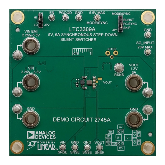
DESCRIPTION
Demonstration Circuit 2745A features the
6A synchronous step-down silent switcher operating as
a 2MHz, 3.3V to 1.2V 6A buck regulator. The LTC3309A
supports adjustable output voltages from 0.5V to V
and operating frequencies from 1MHz up to 3MHz. The
LTC3309A is a compact, ultralow emission, high effi-
ciency, and high speed synchronous monolithic step-
down switching regulator. A minimum on-time of 22ns
enables high V
to low V
IN
switching frequencies.
The DC2745A operating mode may be selected as
Burst Mode
operation, skip or forced continuous (FC)
®
mode. Setting JP1 to the FC/SYNC position will allow
the LTC3309A to sync to a clock frequency from 1MHz
to 3MHz. The LTC3309A operates in forced continuous
mode when syncing to an external clock.
The DC2745A is set to a fixed 2MHz frequency by con-
necting RT to V
through a 0Ω resistor, R9. The frequency
IN
can be easily changed by removing R9 and setting an
appropriate resistor in the R4 location to obtain the
desired frequency. Refer to the LTC3309A data sheet for
the proper RT value for a desired switching frequency.
PERFORMANCE SUMMARY
SYMBOL
PARAMETER
V
Input Voltage Range
IN
V
V
Voltage Range*
OUT
OUT
I
OUTPUT Current
OUT
f
Switching Frequency
SW
t
Top Switch Minimum On Time
ON
Duty Cycle
Top Switch Duty Cycle
*With 1% resistors. Accuracy will improve to within 1% using 0.1% FB resistors.
5V, 6A Synchronous Step-Down
Silent Switcher in 2mm × 2mm LQFN
LTC
3309A
®
conversion ratios at high
OUT
Specifications are at T
CONDITIONS
V
IN
DEMO MANUAL DC2745A
5V,
The DC2745A also has an EMI filter to reduce conducted
EMI. This EMI filter can be included by applying the input
voltage at the V
IN
,
the board is shown in the EMI Test Results section. The
IN
red lines in the EMI performance graphs illustrate the
CISPR25 Class 5 peak limits for the conducted and radi-
ated emission tests.
The LTC3309A data sheet gives a complete description
of the device, operation and application information. The
data sheet must be read in conjunction with this demo
manual. The LTC3309A is assembled in a 2mm × 2mm
LQFN package with exposed pads for low thermal resis-
tance. The layout recommendations for low EMI operation
and maximum thermal performance are available in the
data sheet section Low EMI PCB Layout.
The Efficiency vs Load graph shows the efficiency and
the power loss of the circuit with a 3.3V input in Burst
Mode operation.
Design files for this circuit board are
All registered trademarks and trademarks are the property of their respective owners.
= 25°C
A
Greater than V
OUT
LTC3309A
EMI terminal. The EMI performance of
available.
MIN
TYP
MAX
2.25
1.183
1.2
1.217
1
22
100
UNITS
5.5
V
V
6
A
3
MHz
ns
%
Rev. 0
1
Advertisement
Table of Contents

Related Manuals for Analog Devices DC2745A


Summary of Contents for Analog Devices DC2745A
- Page 1 The Efficiency vs Load graph shows the efficiency and The DC2745A is set to a fixed 2MHz frequency by con- the power loss of the circuit with a 3.3V input in Burst necting RT to V through a 0Ω...
-
Page 2: Circuit Schematic
DEMO MANUAL DC2745A BOARD PHOTO CIRCUIT SCHEMATIC High Efficiency, 2MHz, 1.2V 6A Step-Down Converter LTC3309A 3.3V to 1.2V Efficiency and Powerloss DC2745A in Burst Mode = 2.25V TO 5.5V 1µF 1µF 10µF 10µF 0201 0201 EFFICIENCY 220nH 1.2V 6.8pF 140k 47µF... - Page 3 DEMO MANUAL DC2745A EMI TEST RESULTS CISPR25 Conducted Emisions with Class 5 Peak Limits (Voltage Method) –10 PEAK LIMIT PEAK –20 FREQUENCY (MHz) dc2745a G01 DC2745A DEMO BOARD (WITH EMI FILTER INSTALLED) 3.3V INPUT TO 1.2V OUTPUT AT 4.8A, f...
- Page 4 DEMO MANUAL DC2745A QUICK START PROCEDURE Demonstration circuit 2745A is easy to set up and use duty cycle and the period of the switching waveform to evaluate the performance of the LTC3309A. Refer to (~500nanoseconds). Figure 1 for proper measurement equipment setup and 9.
-
Page 5: Quick Start Procedure
DEMO MANUAL DC2745A QUICK START PROCEDURE Figure 1. Test Setup for the DC2745A Demo Board Rev. 0... - Page 6 DEMO MANUAL DC2745A QUICK START PROCEDURE Figure 2. Technique for Measuring Output Ripple and Step Response a) With a Scope Probe. b) With a Low Inductance Connector (Not Supplied). 6 7 8 SG_INPUT SIR426DP-T1-GE3 20V MAX 1 2 3 RSNS 0.1k...
-
Page 7: Theory Of Operation
The demo board is set up to solder an U.FL, RECEPT, ST SMD, 0Hz to 6GHz 50Ω connector The DC2745A demonstration circuit features the (TP1) near the output cap C4. These pads can also be LTC3309A, a low voltage synchronous step-down silent used to solder a coax cable or other oscilloscope probe switcher. -
Page 8: Parts List
DEMO MANUAL DC2745A PARTS LIST ITEM REFERENCE PART DESCRIPTION MANUFACTURER/PART NUMBER Required Circuit Components CAP ., 0.01µF, X7R, 10V, 10%, 0201 MURATA, GRM033R70J103KA01D C2, C3 CAP ., 10µF, X7S, 6.3V, 20%, 0603 TDK, C1608X7S0J106M080AC C4, C5 CAP ., 47µF, X6S, 6.3V, 20%, 0805 TAIYO YUDEN, JMK212BC6476MG-T CAP ., 6.8pF, C0G/NP0, 50V, ±0.5pF, 0402... -
Page 9: Schematic Diagram
Devices for its use, nor for any infringements of patents or other rights of third parties that may result from its use. Specifications subject to change without notice. No license is granted by implication or otherwise under any patent or patent rights of Analog Devices. - Page 10 Board until you have read and agreed to the Agreement. Your use of the Evaluation Board shall signify your acceptance of the Agreement. This Agreement is made by and between you (“Customer”) and Analog Devices, Inc. (“ADI”), with its principal place of business at One Technology Way, Norwood, MA 02062, USA. Subject to the terms and conditions of the Agreement, ADI hereby grants to Customer a free, limited, personal, temporary, non-exclusive, non-sublicensable, non-transferable license to use the Evaluation Board FOR EVALUATION PURPOSES ONLY.
Need help?
Do you have a question about the DC2745A and is the answer not in the manual?
Questions and answers