Table of Contents
Advertisement
Quick Links
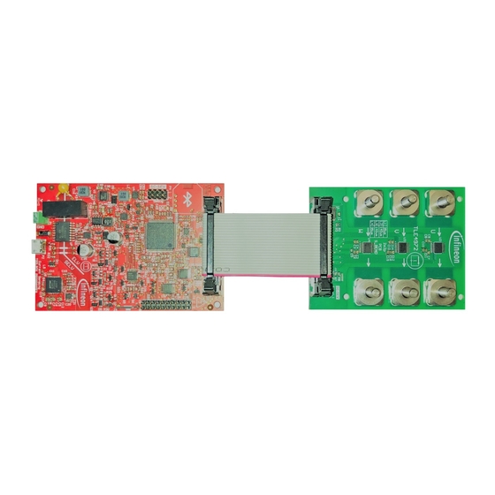
TLE4972 Lateral insertion 45° S-bend on PCB
User guide
About this document
This document describes the evaluation board of TLE4972, Infineon's magnetic current sensor for automotive
applications with external current rail.
Scope and purpose
The evaluation board is meant to be used by the customer solely for the purpose of evaluation and testing. It is
not a commercial product and shall not be used for series production. This board is thus not intend to meet any
industrial specifications and shall be operated at room temperature.
Due to its purpose, the evaluation board is not subject to the same procedures as regular products regarding
Returned Material Analysis (RMA), Process Change Notification (PCN) and Product Withdraw (PWD).
Intended audience
This document is written for customers who intend to use TLE4972 in current sensing applications.
Evaluation Board
This board will be used during design in, for evaluation and measurement of characteristics, and proof of
datasheet specifications.
Note:
PCB and auxiliary circuits are NOT optimized for final customer design. Boards do not necessarily
meet safety, EMI, quality standards (for example UL, CE) requirements.
Figure 1
TLE4972 EVAL STD PCB
User guide
Please read the sections "Important notice" and "Warnings" at the end of this document
www.infineon.com
Rev. 1.00
2022-04-12
Advertisement
Table of Contents

Related Manuals for Infineon TLE4972


Summary of Contents for Infineon TLE4972
- Page 1 Returned Material Analysis (RMA), Process Change Notification (PCN) and Product Withdraw (PWD). Intended audience This document is written for customers who intend to use TLE4972 in current sensing applications. Evaluation Board This board will be used during design in, for evaluation and measurement of characteristics, and proof of datasheet specifications.
-
Page 2: Table Of Contents
TLE4972 Lateral insertion 45° S-bend on PCB User guide Table of contents Table of contents Table of contents ............... 2 Important notice . -
Page 3: Important Notice
Boards provided by Infineon Technologies. The design of the Evaluation Boards and Reference Boards has been tested by Infineon Technologies only as described in this document. The design is not qualified in terms of safety requirements, manufacturing and operation over the entire operating temperature range or lifetime. -
Page 4: Safety Precautions
TLE4972 Lateral insertion 45° S-bend on PCB User guide 2 Safety precautions Safety precautions Note: Please note the following warnings regarding the hazards associated with development systems. Figure 2 Safety Precautions • Warning: Remove or disconnect power from the drive before you disconnect or reconnect wires, or perform maintenance work. -
Page 5: The Board At A Glance
3 The board at a glance The board at a glance TLE4972 evaluation board is developed to familiarize the users with TLE4972 current sensor for design in support and evaluation purposes. The complete evaluation kit consists of this board and the programmer board, which is explained in [1]. - Page 6 TLE4972 Lateral insertion 45° S-bend on PCB User guide 3 The board at a glance Table 1 (continued) Evaluation Board Overview Product TLE4972-AE35D5 Typical evaluation board sensitivity 5.33 mV/A Output mode Semi-differential OCD1 threshold 313.83 A (139% of FS) OCD2 threshold 185.99 A (82% of FS)
-
Page 7: System And Functional Description
Description of the functional blocks The board consists of three TLE4972 current sensors to accurately sense AC and DC currents, a EEPROM to store the board settings, a LDO (Low Drop Out) regulator to stabilize the supply voltage of the sensors and a connector to connect to the Infineon programmer board [1]. -
Page 8: System Design
A voltage regulator is implemented to supply the sensors with a stable voltage. Layout TLE4972 evaluation board consists of two 35 μm outer metallization layers and two 140 μm inner metallization layers. The inner layers are intended to carry the high current that is sensed by the sensors. - Page 9 5 System design Figure 6 Evaluation board layer stack up The figure below shows the top and bottom layer of the evaluation board. Please contact your local Infineon sales office to receive the Gerber files. Figure 7 Evaluation board PCB layout (top and bottom layer) User guide Rev.
-
Page 10: Bill Of Material
Additionally, ground planes are used to protect the signal tracks and reduce the parasitic couplings. The ground and power planes are cut below the TLE4972 including input and output pins to avoid the error induced due to the eddy currents. For the same reason, no heat sink or other conductor material shall be placed on the same position of the sensor. - Page 11 TLE4972 Lateral insertion 45° S-bend on PCB User guide 5 System design Table 3 (continued) Evaluation board connector pinout OCD1_2 Over Current Detection channel 1 of sensor 2 (open drain) VREF2 Reference voltage of sensor 2 OCD2_2 Over Current Detection channel 2 of...
-
Page 12: System Performance
6.2.1.1 Sensitivity drift and offset drift over temperature The figures below show the TLE4972 evaluation board measurement results of sensitivity drift and offset over temperature when the sensor is placed in the nominal position. The results show extremely stable sensitivity and small offset across the whole temperature range. -
Page 13: Frequency Response
6.2.1.2 Frequency response The figures below show the TLE4972 evaluation board measurement results of frequency response (gain and phase) when the sensor is placed in the nominal position. Two out of three sensors have been measured. A comparison with results from Finite Element Method (FEM) simulations is also provided. -
Page 14: Crosstalk
TLE4972 Lateral insertion 45° S-bend on PCB User guide 6 System performance Figure 11 Frequency response (phase) 6.2.1.3 Crosstalk The crosstalk is defined as the sensitivity error due to the magnetic stray field generated by the neighbouring conductive lines. The crosstalk can be compensated with the “Matrix compensation method”... -
Page 15: Thermal Capability
TLE4972 Lateral insertion 45° S-bend on PCB User guide 6 System performance 6.2.1.4 Thermal capability The following figure shows the heating of the board and device when a current flows in the evaluation board. The temperature is read out by the sensor over time and the measurement is stopped when a temperature of approximately 80°C is detected. - Page 16 TLE4972 Lateral insertion 45° S-bend on PCB User guide 6 System performance Figure 13 Conductor resistance, without slit (left) and with slit (right) The table below shows the simulated resistance of the conductor with and without slit and the calculated insertion resistance.
-
Page 17: Transfer Factor Error Due To Sensor Displacement
TLE4972 Lateral insertion 45° S-bend on PCB User guide 6 System performance 6.2.2.2 Transfer factor error due to sensor displacement direction.The transfer factor is defined in μT/A and the typical value is shown in This following figures show the transfer factor variation due to sensor displacement in the x, y, and z-axis Chapter 3.4. - Page 18 TLE4972 Lateral insertion 45° S-bend on PCB User guide 6 System performance Figure 16 Transfer factor error due to sensor displacement in y direction Figure 17 Transfer factor error due to sensor displacement in z direction User guide Rev. 1.00...
-
Page 19: References And Appendices
TLE4972 Lateral insertion 45° S-bend on PCB User guide 7 References and appendices References and appendices Abbreviations and definitions Notation Description Alternating Current European Conformity Direct Current Electro-Magnetic Compatibility Electro-Magnetic Interference EEPROM Electrically Erasable Programmable Read-Only Memory Electro-Static Discharge Finite Element Method... -
Page 20: Revision History
TLE4972 Lateral insertion 45° S-bend on PCB User guide 8 Revision history Revision history Table 6 Revision History Document version Date of release Description of changes 12.04.2022 Initial revision User guide Rev. 1.00 2022-04-12... -
Page 21: Disclaimer
Infineon Technologies, All Rights Reserved. of any kind, including without limitation warranties of Infineon Technologies’ products may not be used in non-infringement of intellectual property rights of any any applications where a failure of the product or third party.
Need help?
Do you have a question about the TLE4972 and is the answer not in the manual?
Questions and answers