Table of Contents
Advertisement
Quick Links
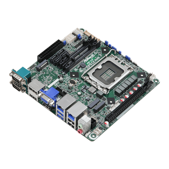
IMB-1230
The terms HDMI
®
and HDMI High-Definition
Multimedia Interface, and the HDMI logo are
trademarks or registered trademarks of HDMI
Licensing LLC in the United States and other
countries.
Revision History
Date
Description
August 10, 2022
First Release
COM Port PWR Setting Jumpers
1 : PWR_COM1 (For COM Port1)
2 : PWR_COM2 (For COM Port2)
7 : PWR_COM3 (For COM Port3)
1-2: +5V
2-3: +12V
3 : ESPI Header
(ESPI1)
4 : M.2 Key-B Socket (M2_B1)
PIN
Signal
Signal
PIN
+3.3V
1
NA
2
+3.3V
3
GND
4
5
GND
FuLL_Card_Power_off
6
7
USB_D+
W_DISABLE
8
9
USB_D-
WWAN_LED#
10
11
GND
21
GND
NA
20
23
NA
NA
22
25
NA
NA
24
27
GND
NA
26
29
USB3_RX-
NA
28
31
USB3_RX+
UIM_RESET
30
33
GND
UIM_CLK
32
35
USB3_TX-
UIM_DATA
34
37
USB3_TX+
UIM_PWR
36
39
GND
NA
38
41
PERn0
NA
40
43
PERp0
NA
42
45
GND
NA
44
47
PETn0
NA
46
49
PETP0
NA
48
51
GND
PERST#
50
53
PEFCLKn
CLKREQ#
52
55
PEFCLKp
NA
54
57
GND
NA
56
59
NA
NA
58
61
NA
NA
60
63
NA
NA
62
65
NA
NA
64
67
NA
NA
66
69
PEDET
NA
68
71
GND
+3.3V
70
73
GND
+3.3V
72
75
NA
+3.3V
74
Jumpers and Headers Setting Guide
5 : 24-pin ATX Power Input Connector
6 : SATA3 Connectors (SATA3_1~4)
8 : SATA Power Output
3 2 1
Connector
9 : COM Port Headers (COM5, 4, 3) (RS232)
COM3:
PWR
RI
RTS
GND
TXD
DCD
1
10 : Digital Input/Output Pin
Header (JGPIO1)
Signal
PIN
Name
10
GND
8
GPP_E6
6
GPP_E5
4
GPP_I10
2
GPP_H23
11 : Backlight Volume Control (BLT_VOL1)
PIN
Signal Name
7
GND
6
GND
5
BLT_DW
4
BLT_UP
3
PWRDN
2
GPIO_VOL_DW
1
GPIO_VOL_UP
12 : Inverter Power Control Wafer (BLT_PWR1)
PIN
Signal Name
6
LCD_BLT_VCC
5
LCD_BLT_VCC
4
CON_LBKLT_EN
3
CON_LBKLT_CTL
2
1
13 : Digital Input / Output Power Select
(JGPIO_PWR1)
1-2: +12V
2-3: +5V
1
13
GND
+5V
1
+12V
GND
COM4, 5:
NC
NC
N/A
RI
CTS
RTS
CTS
GND
DSR
DSR
TXD
DTR
DTR
DCD
RXD
RXD
1
PIN Signal Name
9 JGPIOPWR_R
7
SIO_GP74
5
SIO_GP73
3
SIO_GP72
1
SIO_GP71
1
GND
GND
1
3 2 1
14 : LVDS Panel Connector
12
PIN
Signal Name
PIN
Signal Name
39
LCD_BLT_VCC
40
LCD_BLT_VCC
24
37
CON_LBKLT_CTL
38
LCD_BLT_VCC
35
GND
36
CON_LBKLT_EN
33
LVDS_B_CLK#
34
LVDS_B_CLK
31
LVDS_B_DATA3
32
GND
29
DPLVDD_EN
30
LVDS_B_DATA3#
27
LVDS_B_DATA2#
28
LVDS_B_DATA2
25
LVDS_B_DATA1
26
GND
23
GND
24
LVDS_B_DATA1#
21
LVDS_B_DATA0#
22
LVDS_B_DATA0
19
LVDS_A_CLK
20
GND
17
GND
18
LVDS_A_CLK#
15
LVDS_A_DATA3#
16
LVDS_A_DATA3
13
LVDS_A_DATA2
14
GND
11
GND
12
LVDS_A_DATA2#
9
LVDS_A_DATA1#
10
LVDS_A_DATA1
7
LVDS_A_DATA0
8
GND
5
NA
6
LVDS_A_DATA0#
3
+3.3V
4
NA
1
LCD_VCC
2
LCD_VCC
* eDP by pass mode pin definition
(switch by BIOS):
PIN
Signal Name
39
LCD_BLT_VCC
37
CON_LBKLT_CTL
35
GND
33
N/A
31
N/A
29
DPLVDD_EN
27
N/A
25
N/A
23
GND
21
N/A
19
EDP_AUXP
17
GND
15
N/A
13
EDP_TX0
11
GND
9
EDP_TX1#
7
N/A
5
N/A
3
N/A
1
LCD_VCC
15 : Panel Power Select
(LCD_VCC) (PNL_PWR1)
1-2: LCD_VCC: +3V
2-3: LCD_VCC: +5V
4-5: LCD_VCC: +12V
1
16 : Backlight Power Select
(LCD_BLT_VCC) (BKT_PWR1)
1-2: LCD_BLT_VCC: +5V
2-3: LCD_BLT_VCC: +12V
17 : CON_LBKLT_CTL Voltage Level
(BLT_PWM2)
1-2: 3V Level
2-3: 5V Level
39
40
1
2
PIN
Signal Name
40
LCD_BLT_VCC
38
LCD_BLT_VCC
36
CON_LBKLT_EN
34
N/A
32
GND
30
N/A
28
N/A
26
GND
24
N/A
22
N/A
20
GND
18
EDP_AUXN
16
N/A
14
GND
12
EDP_TX0#
10
EDP_TX1
8
GND
6
N/A
4
N/A
2
LCD_VCC
Advertisement
Table of Contents

Subscribe to Our Youtube Channel
Related Manuals for ASRock Industrial IMB-1230


Summary of Contents for ASRock Industrial IMB-1230
- Page 1 Jumpers and Headers Setting Guide IMB-1230 The terms HDMI ® and HDMI High-Definition Multimedia Interface, and the HDMI logo are trademarks or registered trademarks of HDMI Licensing LLC in the United States and other countries. Revision History Date Description August 10, 2022...
- Page 2 Installation of ROM Socket * Do not apply force to the actuator cover after ic inserted. * Do not apply force to actuator cover when it is opening over 120 degree, Otherwise, the actuator cover may be broken. * The yellow dot (Pin1) on the ROM must be installed at pin1 position of the socket (white arrow area).
Need help?
Do you have a question about the IMB-1230 and is the answer not in the manual?
Questions and answers