Table of Contents
Advertisement
Quick Links
Data Sheet
May 2012
The DS3106DK is an easy-to-use demo and
evaluation kit for the DS3106 line card timing IC. A
surface-mounted DS3106 and careful layout provide
maximum
signal integrity.
compatible microcontroller and included software
give point-and-click access to configuration and
status registers from a Windows®-based PC. LEDs
on
the
board
indicate
function,
and
lock
differential clocks are accessed via SMB connectors.
All LEDs and connectors are clearly labeled with
silkscreening to identify associated signals.
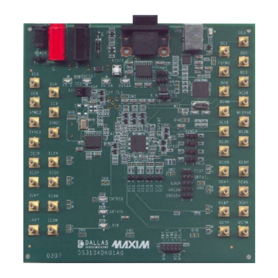
DS3106DK Board
CD-ROM Includes:
DS3106 Software
DS3106 Initialization File
DS3106DK Data Sheet
DS3106 Data Sheet/Errata Sheet
Windows is a registered trademark of Microsoft Corp.
General Description
An on-board 8051-
interrupt,
power-supply
status.
Single-ended
Demo Kit Contents
DS3106DK Demo Kit
Evaluates: DS3106 Timing IC
♦
Soldered DS3106 for Best Signal Integrity
♦
SMB Connectors and Termination Ease
Connectivity
♦
Careful Layout for Analog Signal Paths
♦
On-Board Stratum 3 Oscillator with Footprints
for Stratum 3E and Stratum 4 Oscillators
♦
On-Board Microcontroller and Included
and
Software Provide Point-and-Click Access to
the DS3106 Register Set
♦
LEDs for Interrupt, Power Supplies, and Lock
Status
♦
Banana Jack VDD and GND Connectors
Support Use of Lab Power Supplies
♦
Easy-to-Read Silkscreen Labels Identify the
Signals Associated with All Connectors,
Jumpers, and LEDs
♦
Software Provides GUI Fields for Most
Commonly Used Features Plus Full
Read/Write Access to the Entire Register Set
♦
Software Support for Creating and Running
Configuration Scripts Saves Time During
Evaluation
Minimum System Requirements
♦
PC Running Windows XP or Windows 2000
♦
Display with 1024 x 768 Resolution or Higher
♦
Available USB or Serial (COM) Port
♦
USB Cable or DB-9 Serial Cable
PART
DS3106DK
Features
Ordering Information
DESCRIPTION
Demo kit for DS3106
1
Advertisement
Table of Contents

Related Manuals for Microsemi DS3106DK


Summary of Contents for Microsemi DS3106DK
- Page 1 Evaluates: DS3106 Timing IC General Description Features ♦ Soldered DS3106 for Best Signal Integrity The DS3106DK is an easy-to-use demo and evaluation kit for the DS3106 line card timing IC. A ♦ SMB Connectors and Termination Ease surface-mounted DS3106 and careful layout provide...
-
Page 2: Table Of Contents
_________________________________________________________________________________________ DS3106DK Table of Contents BOARD FLOORPLAN ........................4 ......................5 NPUT AND UTPUT LOCKS ................. 5 UMPERS EADERS WITCH ETTINGS ........................5 ICROCONTROLLER ..................... 5 OWER UPPLY ONNECTORS BASIC HARDWARE SETUP ......................6 USB D ......................6 RIVER NSTALLATION INSTALLING AND RUNNING THE SOFTWARE ................ - Page 3 _________________________________________________________________________________________ DS3106DK List of Figures Figure 1-1. DS3106DK Board Floorplan ........................4 Figure 4-1. Software Main Screen ..........................8 Figure 4-5. Software-Programmable DFS Window ....................13 Figure 4-6. Software I/O Pins Window ........................14 Figure 4-7. Software Register View Window ......................15 List of Tables Table 4-1.
-
Page 4: Board Floorplan
JTAG connector and LED indicators. The DS3106DK has the same PCB design as demo kits for timing ICs with more clock I/Os. As a result, many of the connectors are not populated in the DS3106DK. See Appendix 1: Hardware Components for a complete component list. -
Page 5: Input And Output Clocks
Jumper JMP6 (labeled VDDIOB) is not used in the DS3106DK. Jumpers JMP62 and JMP63 select the computer interface to be USB or RS232. Jumper JMP5 (upper left) selects whether the board should be powered from the USB connector or from the power-supply jacks (J3 or J13/J19). -
Page 6: Basic Hardware Setup
4) Repeats steps 1 to 3 the second time the Found New Hardware Wizard starts. After the drivers are installed, whenever the DS3106DK board is connected to a USB port on the PC, the Windows operating system will see the USB-to-serial converter IC as an additional COM port. The DS3106DK software will automatically list the additional COM port in the PORT selection combo box in the upper-left corner of the main window. -
Page 7: Installing And Running The Software
At this time the DS3106 demo kit software only runs on Windows 2000 or Windows XP operating systems. To install the demo kit software, run SETUP.EXE from the disk included in the DS3106DK box or from the zip file available on the Microsemi website or from Microsemi timing products technical support. -
Page 8: Overview Of The Software Interface
_________________________________________________________________________________________ DS3106DK Overview of the Software Interface Figure 4-1. Software Main Screen Global Configuration In the upper-left corner of the main window are several global status and configuration fields. The ID field displays the device part number and revision. The PORT field shows the COM port to which the DK board is connected. -
Page 9: T0 Dpll
_________________________________________________________________________________________ DS3106DK Table 4-1. Mapping Between Input Clock Software Fields and DS3106 Register Fields SOFTWARE FIELD DS3106 REGISTER FIELDS ISR2 register LED red when ACT = 1, LOCK = 0 Input Clock Status LEDs 3 and 4 LED green when ACT = 0, LOCK = 0... -
Page 10: T0 Apll And T0 Apll2
_________________________________________________________________________________________ DS3106DK T0 APLL and T0 APLL2 The Input Freq field configures the frequency of the T0 APLL DFS (refer to the DS3106 data sheet for details). The APLL output frequency is always four times the input frequency. When the Input Freq field is changed, the Output Freq field changes to match, and all the T0 options in the OC3 and OC6 output clock combo boxes also change to frequencies derived from the new T0 APLL frequency. -
Page 11: Dpll Frequency Limits, Phase Detectors, Dpll Lock Criteria
_________________________________________________________________________________________ DS3106DK DFS are configured for programmable DFS operation, the DIG1 and DIG2 fields change to display the programmable DFS frequency with a “P” prefix. FSYNC is an 8kHz output that can be configured as a 50% duty cycle clock or a frame pulse and can optionally be inverted. -
Page 12: Programmable Dfs
_________________________________________________________________________________________ DS3106DK Programmable DFS When the Programmable DFS button in the upper-right corner of the main window is pressed, the Programmable DFS window appears (Figure 4-2). In this window one or more of the output DFS engines in the DS3106 can be configured to synthesize a custom frequency that is a multiple of 2kHz (f <... - Page 13 _________________________________________________________________________________________ DS3106DK Figure 4-2. Software-Programmable DFS Window...
-
Page 14: I/O Pins
_________________________________________________________________________________________ DS3106DK 4.10 I/O Pins The fields in this window configure the general-purpose I/O available on the DS3106. See Figure 4-3, Table 4-8, and the DS3106 data sheet for details. Figure 4-3. Software I/O Pins Window Table 4-8. Mapping Between I/O Pins Software Fields and DS3106 Register Fields... -
Page 15: Register View Window
_________________________________________________________________________________________ DS3106DK 4.11 Register View Window When the Register View button in the upper-right corner of the main window is pressed, the Register View window appears (Figure 4-4). In this window the DS3106’s entire register set can be viewed and manually written as needed. -
Page 16: Configuration Scripts And Log File
4.12.1 Configuration Log File Every write command issued by the software to the DS3106DK board is logged in file DS3106DKLog.mfg located in the same directory as the software executable. This file can be viewed in Notepad by pressing the Log File button in the upper-right corner of the main window. -
Page 17: Appendix 1: Hardware Components
_________________________________________________________________________________________ DS3106DK Appendix 1: Hardware Components DESIGNATION DESCRIPTION SUPPLIER PART C1, C2, C5, C6, C9–C12, C15, C42, C59–C138, C140, 0.1µF ±20% 16V X7R ceramic capacitors (0603) C142, C143, C145, 0603YC104MAT C147, C151, C155, C163–C166, C168, C169 C3, C13 ,C14, C16, 4.7µF ±10%, 25V X5R ceramic capacitors (1206) - Page 18 _________________________________________________________________________________________ DS3106DK DESIGNATION DESCRIPTION SUPPLIER PART R5, R11, R13, R15, R21–R24, R29–R32, L_RES 0603 51.1 Ohm 1/16W 1% ERJ-3EKF51R1V R65–R68 RES 0603 100K Ohm 1/16W 5% ERJ-3GEYJ104V R7, R9, R10, R12, R14, R84, R110, L_RES 0603 10K Ohm 1/16W 5%...
-
Page 19: Appendix 2: Schematics
3.3V CMOS, LOW JITTER-12.8MHz, 4-PIN S1633A-12.8000 SMD, DO NOT POPULATE XTAL, LOW PROFILE, 11.0592MHz LP49-33-11.0592M Appendix 2: Schematics The schematics are featured in the following pages. Document Revision History REVISION DESCRIPTION DATE 012208 Initial release. 2012-05 Reformatted for Microsemi. No content change. - Page 22 JMP2 JMP3 JMP4 R102...
- Page 32 Microsemi Corporate Headquarters © 2012 Microsemi Corporation. All rights reserved. Microsemi and the Microsemi logo are trademarks of One Enterprise, Aliso Viejo CA 92656 USA Microsemi Corporation. All other trademarks and service marks are the property of their respective owners.
Need help?
Do you have a question about the DS3106DK and is the answer not in the manual?
Questions and answers