Table of Contents
Advertisement
Quick Links
Advertisement
Table of Contents

Related Manuals for Microsemi LX7175


Summary of Contents for Microsemi LX7175
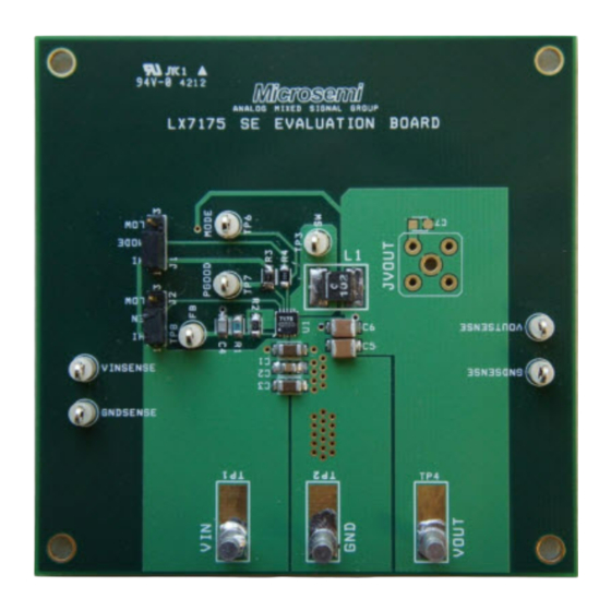
- Page 1 LX7175 User Guide LX7175 3 Amp Step-Down Converter Evaluation Board...
-
Page 2: Table Of Contents
LX7175 3 Amp Step-Down Converter Evaluation Board Contents 1 Revision History ..........................1 1.1 Revision 1.0 ............................1 2 Product Description ........................2 2.1 Applications ............................2 2.2 Key Features ............................2 3 Evaluation Board Schematic ......................3 4 Basic Connection Instructions ......................4 5 Recommended Operating Conditions .................... -
Page 3: Revision History
LX7175 3 Amp Step-Down Converter Evaluation Board Revision History The revision history describes the changes that were implemented in the document. The changes are listed by revision, starting with the most current publication. Revision 1.0 Revision 1.0 was published in August 2017. It was the first publication of this document. -
Page 4: Product Description
The operational input voltage range of the LX7175 is from 3 V to 5.5 V and it has two modes of operation selected externally by the MODE pin. When the MODE pin is high, the device operates in continuous PWM operation, and when it is tied low, it operates in power wave mode (PSM) with automatic transition between PWM and PSM mode depending on the load current. -
Page 5: Evaluation Board Schematic
LX7175 3 Amp Step-Down Converter Evaluation Board Evaluation Board Schematic The following illustration shows the evaluation board schematic. Figure 1 • Schematic of Evaluation Board LX7175 User Guide Revision 2.0... -
Page 6: Basic Connection Instructions
LX7175 3 Amp Step-Down Converter Evaluation Board Basic Connection Instructions The following illustration shows how to connect the evaluation board to the power supply. Figure 2 • Power Supply and Load Connection LX7175 User Guide Revision 2.0... -
Page 7: Recommended Operating Conditions
LX7175 3 Amp Step-Down Converter Evaluation Board Recommended Operating Conditions The following table lists the operating conditions for the LX7175 Evaluation Board. Table 1 • Operating Conditions Description Symbol Minimum Maximum Unit Input voltage Output current Operating ambient temperature –10 °C... -
Page 8: Pcb Layout Of Evaluation Board
LX7175 3 Amp Step-Down Converter Evaluation Board PCB Layout of Evaluation Board The LX7175 Evaluation Board is a four-layer board. The following illustrations depict each of the board's four layers. Figure 3 • Top Silkscreen LX7175 User Guide Revision 2.0... - Page 9 LX7175 3 Amp Step-Down Converter Evaluation Board Figure 4 • Layer 1: Top Layer LX7175 User Guide Revision 2.0...
- Page 10 LX7175 3 Amp Step-Down Converter Evaluation Board Figure 5 • Layer 2: Inner Layer 1 LX7175 User Guide Revision 2.0...
- Page 11 LX7175 3 Amp Step-Down Converter Evaluation Board Figure 6 • Layer 3: Inner Layer 2 LX7175 User Guide Revision 2.0...
- Page 12 LX7175 3 Amp Step-Down Converter Evaluation Board Figure 7 • Layer 4: Bottom Layer LX7175 User Guide Revision 2.0...
-
Page 13: Bill Of Materials
LX7175 3 Amp Step-Down Converter Evaluation Board Bill of Materials The following table lists the bill of materials (BOM) for the LX7175 Evaluation Board. Table 2 • BOM Item Part Type Specification Reference Quantity Miscellaneous Microsemi IC—LX7175 component Miscellaneous Test point... -
Page 14: Efficiency Plot
LX7175 3 Amp Step-Down Converter Evaluation Board Efficiency Plot The following graph shows the efficiency of the LX7175 at a voltage output of 1 V. Figure 8 • Efficiency Plot of LX7175 LX7175 User Guide Revision 2.0... -
Page 15: Dynamic Load Response Scope Shots
LX7175 3 Amp Step-Down Converter Evaluation Board Dynamic Load Response Scope Shots The following graph shows the board's dynamic load response, PWM. Figure 9 • Dynamic Load Response With 1 A–3 A Load, PWM CH2: VOUT, CH4: load current LX7175 User Guide Revision 2.0... -
Page 16: Start-Up Scope Shots
LX7175 3 Amp Step-Down Converter Evaluation Board Start-up Scope Shots The following graphs show the scope shots for the LX7175. 10.1 Start-up with Enable Toggled The following graph shows startup with ENABLE toggled. Figure 10 • Start-up with ENABLE Toggled CH1: V , CH2: V , CH3: PGOOD, CH4: inductor current. -
Page 17: Power-Up With No Load (En Tied To 5 V Vin, Pwm)
LX7175 3 Amp Step-Down Converter Evaluation Board 10.2 Power-up with No Load (EN Tied to 5 V VIN, PWM) The following graph shows power-up with no load. Figure 11 • Power-up with No Load CH1: V , CH2: V , CH3: PGOOD, CH4: inductor current. -
Page 18: Power-Up With Resistive Load (En Tied To 5 V Vin, Pwm)
LX7175 3 Amp Step-Down Converter Evaluation Board 10.3 Power-up with Resistive Load (EN Tied to 5 V VIN, PWM) The following graph shows power-up with resistive load. Figure 12 • Power-up with Resistive Load (EN Tied to 5 V VIN, PWM) CH1: V , CH2: V , CH3: PGOOD, CH4: inductor current. -
Page 19: Power-Up With No Load (En Tied To 5 V Vin, Psm)
LX7175 3 Amp Step-Down Converter Evaluation Board 10.4 Power-up with No Load (EN Tied to 5 V VIN, PSM) The following graph shows power-up with no load. Figure 13 • Power-up with No Load (EN Tied to 5 V VIN, PSM) CH1: V , CH2: V , CH3: PGOOD, CH4: inductor current. -
Page 20: Ordering Information
LX7175 3 Amp Step-Down Converter Evaluation Board Ordering Information The following table lists the ordering information for the LX7175 evaluation board and IC. Table 3 • Ordering Information Part Order Number Description LX7175CLD DFN 3 mm × 3 mm 10-layer integrated circuit... - Page 21 Microsemi. It is the Buyer's responsibility to independently determine suitability of any products and to test and verify the same. The information provided by Microsemi hereunder is provided "as is, where is" and with all faults, and the Microsemi Corporate Headquarters entire risk associated with such information is entirely with the Buyer.
Need help?
Do you have a question about the LX7175 and is the answer not in the manual?
Questions and answers