Table of Contents
Advertisement
Quick Links
Advertisement
Table of Contents

Subscribe to Our Youtube Channel
Related Manuals for Motorola M68360QUADS-040


Summary of Contents for Motorola M68360QUADS-040
- Page 1 Freescale Semiconductor, Inc. MICROPROCESSOR & MEMORY MOTOROLA TECHNOLOGIES GROUP M68360QUADS-040 User’s Manual ISSUE 1.0 - DRAFT SIX SIGMA 6 σ For More Information On This Product, Go to: www.freescale.com MOTOROLA Thi d t d ith F M k 4 0 4...
-
Page 2: Table Of Contents
INSTALLATION INSTRUCTIONS 2.4.1 +5V Power Supply Connection 2.4.2 P7: +12V Power Supply Connection 2.4.3 ADI Installation 2.4.4 Host computer to M68360QUADS-040 Connection 2.4.5 Terminal to M68360QUADS-040 RS-232 Connection OPERATING INSTRUCTIONS INTRODUCTION CONTROLS AND INDICATORS 3.2.1 SOFT RESET Switch SW1 3.2.2 ABORT Switch SW2 3.2.3... - Page 3 Freescale Semiconductor, Inc. M68360QUADS-040 - User’s Manual TABLE OF CONTENTS Programming the slave QUICC 3.4.1 Module Base Address Register 3.4.2 Module Configuration Register 3.4.3 CLKO Control Register 3.4.4 PLL Control Register 3.4.5 Port E Pin Assignment Register 3.4.6 System Protection Control 3.4.7...
- Page 4 ADI Installation in the SUN-4 APPENDIX B - ADI PORT HANDSHAKE DESCRIPTION INTRODUCTION ADI Port Concept and Operation Description Handshake Description B.3.1 Write Cycle from Host to M68360QUADS-040 B.3.2 Write Cycle from M68360QUADS-040 to Host B.3.3 M68360QUADS-040 Interrupt to the Host B.3.4 Host Interrupt to the M68360QUADS-040 B.3.5...
- Page 5 Physical Location of jumper JG1 and JG2 FIGURE A-2 JG1 Configuration Options FIGURE A-3 ADI board for SBus FIGURE B-1 Host Computer (ADI) to M68360QUADS-040 Connection 56 FIGURE B-2 Host Write to M68360QUADS-040 FIGURE B-3 M68360QUADS-040 Write Cycle to Host FIGURE B-4 M68360QUADS-040 Interrupt to Host Draft 1.0...
- Page 6 M68360QUADS-040 User’s Manual LIST OF TABLES TABLE 1-1. M68360QUADS-040 Specifications TABLE 3-1. EC040 Cycle Types and Responding Devices TABLE 3-2 M68360QUADS-040 Main Memory Map TABLE 4-1. DRAM SIMM Types TABLE 4-2 Port A Pins Description TABLE 4-3 Port B Pins Description...
-
Page 7: General Information
This document describes the evaluation board for the MC68EC040 - MC68360 combination called the M68360QUADS-040. This board is constructed with an MC68EC040 as the master processor and a MC68360 (QUICC) as a slave in MC68EC040 companion mode. The purpose of this board is to evaluate the performance of the above combination, rather than serve as a development system. -
Page 8: Cooling Requirements
The 12V supply is not used on the board, it is connected only to the Ethernet AUI connectors P3 & P5 to be supplied to the network. Therefore, the power consumption of that supply is independent of the M68360QUADS-040. -
Page 9: Features
Serial RS-232 port for terminal or host computer connection via 9 pin Dtype connector. Two Ethernet ports: 1. The first using Motorola’s MC68160 (EEST) with both AUI and TP connectors. 2. The second using AMD’s Am7992 (SIA) with AUI connector. -
Page 10: Hardware Block Diagram
Freescale Semiconductor, Inc. M68360QUADS-040 Hardware User’s Manual GENERAL INFORMATION 5. Dual-port Ethernet controller. VMEbus double-height board dimensions SOFT-RESET, HARD-RESET and ABORT switches. Status LEDs for power, EC040 run, DMA run, HALT and Ethernet signals. Single +5Vdc power supply. HARDWARE BLOCK DIAGRAM... -
Page 11: Hardware Preparation And Installation
DAMAGE CIRCUITS. HARDWARE PREPARATION To select the desired configuration and ensure proper operation of the M68360QUADS-040 board, changes of the Dip-Switch settings may be required before installation. The location of the switches, LEDs, Dip-Switches, and connectors is illustrated in FIGURE 2-1. The board has been factory tested and is shipped with Dip-Switch settings as described in the following paragraphs. -
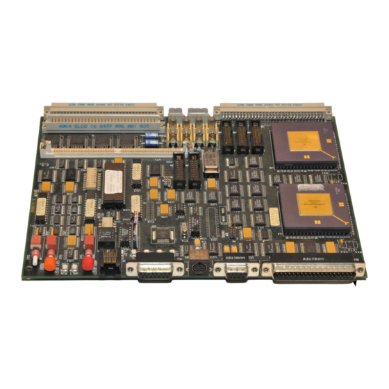
Page 12: Figure 2-1 M68360Quads Location Diagram
Freescale Semiconductor, Inc. M68360QUADS-040 Hardware User’s Manual Hardware Preparation and Installation FIGURE 2-1 M68360QUADS Location diagram SOFT RESET ABORT For More Information On This Product, Go to: www.freescale.com... -
Page 13: Adi Port Address Selection
2.3.1 ADI Port Address Selection The M68360QUADS-040 can have eight possible slave addresses set for its ADI port, enabling up to eight M68360QUADS-040 boards to be connected to the same ADI board in the host computer. The selection of the slave address is done by setting switches 6, 7 & 8 in the Dip-Switch. Switch 6 stands for the most- significant bit of the address and switch 8 stands for the least-significant bit. -
Page 14: Caches Enable / Disable
For further information on that subject see 4.11.5 on page 35. INSTALLATION INSTRUCTIONS When the M68360QUADS-040 has been configured as desired by the user, it can be installed according to the required working environment as follows: For More Information On This Product,... -
Page 15: Power Supply Connection
The M68360QUADS-040 requires +12 Vdc @ 1 A max, power supply for the Ethernet AUI port. The M68360QUADS-040 can work properly without the +12V power supply, if the AUI port is not in use or if the AUI port is used with an AUI hub that does not require 12 V to be provided by the network termination equipment. -
Page 16: Terminal To M68360Quads-040 Rs-232 Connection
HOST_BRK~ ADS_BRK N.C. NOTE: Pin 26 on the ADI is connected to +12 v power supply, but it is not used in the M68360QUADS-040. 2.4.5 Terminal to M68360QUADS-040 RS-232 Connection In the stand-alone operation mode, a VT100 compatible terminal should be connected to the RS-232 connector P2. -
Page 17: Operating Instructions
3.2.1 SOFT RESET Switch SW1 The SOFT RESET switch, SW1, resets all M68360QUADS-040 devices, and resets the EC040, and performs soft reset to the QUICC internal modules, maintaining QUICC’s configuration (clocks & chip- selects) . The switch signal is debounced, and it is not possible to disable it by software. -
Page 18: Tpfuldl Jumper - J5
Bus Grant Input of the EC040, allowing for an external (off-board) arbiter to be located between them. NOTE For proper operation of the M68360QUADS-040, BOTH J9 and J10 must be In Position, unless an external arbiter is connected via the expansion connectors. -
Page 19: Dmarun Indicator - Ld9
Freescale Semiconductor, Inc. M68360QUADS-040 Hardware User’s Manual OPERATING INSTRUCTIONS 3.2.11 DMARUN Indicator - LD9 The yellow DMARUN indicator is connected to AS* signal of the slave QUICC, this to indicate bus activity of one of the QUICC’s DMA channels. 3.2.12... -
Page 20: Main Memory Map
2. The device appears repeatedly in multiples of its size. For example, the Status Register appears at memory locations 01230002, 01230006, 012300A etc... 3. The DRAM SIMM installed in the M68360QUADS-040 is MCM36256 256Kx36 bit. The user may replace the DRAM module with a higher density SIMM and increase the DRAM space up to 8 MBytes. -
Page 21: Programming The Slave Quicc
Freescale Semiconductor, Inc. M68360QUADS-040 Hardware User’s Manual OPERATING INSTRUCTIONS Programming the slave QUICC The slave QUICC (core disabled) provides the following functions on the M68360QUADS-040: 1. DRAM Controller 2. Chip Select and DSACK~ generator. 3. Parallel port (ADI). 4. UART for terminal or host computer connection. -
Page 22: Global Memory Register
• Base address 400000. • Burst support for EC040 access • Parity disabled OR1 must be initialized according to the type of the DRAM SIMM installed on the M68360QUADS-040 as follows: For More Information On This Product, Go to: www.freescale.com... -
Page 23: Base Register 2 And Option Register 2
Base register 2 (BR2) and Option register 2 (OR2) control the operation of RAS2~ pin of the slave QUICC. This pin is connected to the second bank of the DRAM module. BR2 must be initialized according to the type of DRAM SIMM installed on the M68360QUADS-040 as follows: •... -
Page 24: Base Register 5 And Option Register 5
PADAT for that pin is driven onto the pin. On the M68360QUADS-040, port A is used for serial channels as well as for ADI parallel port. PADAT must be initialized to ’3F00’ before configuring the other port registers. -
Page 25: Port B Data Direction Register
Freescale Semiconductor, Inc. M68360QUADS-040 Hardware User’s Manual OPERATING INSTRUCTIONS 3.4.22 Port B Data Direction Register The port B data direction register (PBDIR) has different functions according to the configuration of the port pins. If a pin is general purpose I/O pin, the value in the PBDIR for that pin defines the direction of the pin. -
Page 26: Functional Description
Master MC68EC040 The CPU on the M68360QUADS-040 is a 33 MHz MC68EC040, running at 25 MHz, which uses the slave QUICC’s “68EC040 companion mode” as the memory controller, the interrupt controller, bus arbiter and other system functions usually provided by dedicated logic or peripherals. Due to this “companion” mode support, the MC68EC040 interfaces gluelessly to the QUICC, while some of the QUICC pins change their function to match these of the 68EC040. -
Page 27: Utilizing The Mc68Ec040 Data Cache
Since the bus interface of the EC040 and the QUICC’s DMA are different, snooping is not supported on the M68360QUADS-040. Therefore, when the Data cache is enabled and used, two basic problems arise: 1. When registers or buffer descriptors are changed values by hardware or DMA are to be polled, they should not be cached, otherwise they will be polled indefinitely from the data cache, while their value may change outside, unnoticed by application software. -
Page 28: Host - Nmi
4.3.2 Host - NMI When a host is connected to the M68360QUADS-040 via the ADI port, it is possible for the host to generate a level - 7 interrupt via the ADI port, allowing for full remote control over the board. To generate that interrupt, the host computer needs to assert and deassert the ADS_BRK signal of the ADI port. -
Page 29: System Utilities
BCLRO~ signal of the QUICC is not used. In sake of simplicity, no use is done with the IPEND~ is not used as a BCLI~ for the QUICC. System Utilities The slave QUICC provides the M68360QUADS-040 with the following system utilities, usually provided by external logic: 1. Breakpoint generation 2. -
Page 30: Spurious Interrupt Monitor
4.5.4 software Watch-Dog The software watch-dog on the M68360QUADS-040 may be programmed to generate a system reset when an application software is stuck in an endless loop. The software watch dog is disabled after reset and it may be enabled if the users want it enabled. -
Page 31: Eeprom
4.10 DRAM The M68360QUADS-040 is supplied with 1 Mbyte of Dynamic RAM, which is implemented by the MCM36256S-60 DRAM module. The module is a 72 lead SIMM, 60 nsec access time, organized as 256K x 36 bit for data and parity signals, and is accessed with 3,2,2,2 clock cycles during burst cycles and 3 clocks during normal read / write access. -
Page 32: Dram Controller
The slave QUICC device provides the necessary control signals for the DRAM module. The debugger on the M68360QUADS-040 reads the presence detect pins (SIMM1 - SIMM4) of the SIMM found in the status register and sets the DRAM Controller parameters according to the DRAM module’s size and access time. -
Page 33: Adi Port Signal Description
HOST_BRK~ ADS_BRK N.C. NOTE: Pin 26 on the ADI is connected to +12 v power supply, but it is not used in the M68360QUADS-040. 4.11.3.1 ADI Port Signal Description The ADI port on the QUADS-040 was slightly modified to generate either hard reset or soft reset. This feature was added to comply with the QUICC’s reset mechanism. -
Page 34: Rs-232 Serial Port
4.11.4 RS-232 Serial Port The serial port is provided by one of the slave QUICC serial channels. The M68360QUADS-040 can be connected to a VT100 compatible terminal or to a host computer through the serial port. For More Information On This Product,... -
Page 35: Rs-232 Port Signal Description
N.C. 4.11.4.1 RS-232 Port Signal Description In the list below, the directions ’I’, ’O’, and ’I/O’ are relative to the M68360QUADS-040 board. (I.E. ’I’ means input to the M68360QUADS-040) • CD ( O ) - Data Carrier Detect. This line is always asserted by the ADS. -
Page 36: Ethernet Controller
OPT2* - When active ’1’, indicates that switch #3 in DSW1 is in ON position 4.11.6 Ethernet Controller There are TWO ethernet ports on the M68360QUADS-040 implemented via SCC1 and SCC2 of the QUICC. The first Ethernet port is implemented by connecting SCC1 to Motorola’s MC68160 EEST device. The MC68160 provides two Ethernet interfaces: AUI (P3) and Twisted-Pair (P4). -
Page 37: Ethernet Twisted-Pair Port Signal Description
SPI port of the slave QUICC (pins 1,2 and 3 of port B), and by a general purpose output pin (pin 0 of port B). The SPI port operates in master mode. The serial EEPROM serves as non-volatile memory on the M68360QUADS-040 and may be used to store software parameters to be protected from power-downs. -
Page 38: Slave Quicc Port B
Freescale Semiconductor, Inc. M68360QUADS-040 Hardware User’s Manual FUNCTIONAL DESCRIPTION Port A is 16 pins port. TABLE 4-2 describes the configuration of port A. TABLE 4-2 Port A Pins Description Pin Name Description EEST RX This pin is connected to the receive data output of the EEST. It is configured as the receive data of SCC1 in the slave QUICC. -
Page 39: Slave Quicc Port C
Freescale Semiconductor, Inc. M68360QUADS-040 Hardware User’s Manual FUNCTIONAL DESCRIPTION Port B is 18 pins port. TABLE 4-2 describes the configuration of port B. TABLE 4-3 Port B Pins Description Pin Name Description EEPROM This pin is connected to the select input of the EEPROM, and it is configured as Select output pin in the slave QUICC. -
Page 40: Slave Quicc Port E
Freescale Semiconductor, Inc. M68360QUADS-040 Hardware User’s Manual FUNCTIONAL DESCRIPTION Port C is 12 pins port. TABLE 4-2 describes the configuration of port C. TABLE 4-4 Port C Pins Description Pin Name Description EEST TENA This pin is connected to the TENA input of the EEST. It is configured as the RTS signal of SCC1 in the slave QUICC. -
Page 41: Support Information
96 pin DIN connectors for off-board hardware expansions. 5.2.1 Connector P1 Interconnect Signals Connector P4 is a 37 pin, male D-type connector. It is the ADI port of the M68360QUADS-040. TABLE 5- 1 describes the P1 connector signals. TABLE 5-1 Connector P1 Interconnect Signals Pin No. -
Page 42: Connector P2 Interconnect Signals
Bit 6 of the ADI port data bus 5.2.2 Connector P2 Interconnect Signals Connector P2 is a 9 pin, female D type connector. It is the RS-232 serial port of the M68360QUADS-040. TABLE 5-1 describes the P5 connector signals. TABLE 5-2 Connector P2 Interconnect Signals Pin No. -
Page 43: Connector P4 Interconnect Signals
Ground signal of the M68360QUADS-040. Not connected 5.2.4 Connector P4 Interconnect Signals Connector P4 is 8 pin, RJ-45 connector. It is the twisted-pair Ethernet port of the M68360QUADS-040 board. TABLE 5-1 describes the P8 connector signals. TABLE 5-4 Connector P8 Interconnect Signals Pin No. -
Page 44: Connector P6 Interconnect Signals
SUPPORT INFORMATION TABLE 5-5 Connector P5 Interconnect Signals Pin No. Signal Name Description ARX+ Receive Data positive input to the M68360QUADS-040. Ground signal of the M68360QUADS-040. Not connected Ground signal of the M68360QUADS-040. ACX- Collision detect negative input to the M68360QUADS-040. -
Page 45: Connector P9 Interconnect Signals
Freescale Semiconductor, Inc. M68360QUADS-040 Hardware User’s Manual SUPPORT INFORMATION TABLE 5-8 Connector P8 Interconnect Signals Pin No. Signal Name Description Transfer Type signal 0 pin of the EC040 M68360QUADS-040 board Ground. C6 - C7 SIZ0 - SIZ1 EC040’s Access Size indicators 0 to 1 BRQ~ Quicc’s Bus Request... - Page 46 Freescale Semiconductor, Inc. M68360QUADS-040 Hardware User’s Manual SUPPORT INFORMATION TABLE 5-9 Connector P9 Interconnect Signals Pin No. Signal Name Description SIA_TX SIA Transmit Data. Also SCC2’s Transmit Data A5 - A6 Board’s GND A7 - A8 PA6 - PA7 Port A 6 - 7 Parallel I/O lines Board’s Ground...
-
Page 47: Connector P10 Interconnect Signals
It is identical in pin out to P9. For interconnect signal reference, see TABLE 5-1 on page 41. M68360QUADS-040 Parts List The components of the M68360QUADS-040 and their reference designation are listed in TABLE 5-10. TABLE 5-10 Parts List Reference... - Page 48 Connector 96 pin DIN male straight Logic analyzer P10, P11 Connector 96 pin DIN female 90 . Compatible wire-wrap Expansion connectors are supplied with the M68360QUADS-040. Resistor 39.1 Ω R1 - R3, R12 - R14, R18 - R21 R4, R11, R17, Resistor 4.7 KΩ...
- Page 49 Freescale Semiconductor, Inc. M68360QUADS-040 Hardware User’s Manual SUPPORT INFORMATION TABLE 5-10 Parts List Reference Part Description Notes Designation Resistor 100 Ω Resistor 150 Ω R25 - R28 Resistor network 16 pin, 8 resistors 22 Ω RN1 RN2 RN3 - RN10 Resistor network 14 pin, 13 resistors 4.7 KΩ...
- Page 50 Freescale Semiconductor, Inc. M68360QUADS-040 Hardware User’s Manual SUPPORT INFORMATION For More Information On This Product, Go to: www.freescale.com...
-
Page 51: Introduction
The ADI board should be installed in one of the IBM-PC/XT/AT motherboard system expansion slots. A single ADI can control up to eight M68360QUADS-040 boards. The ADI address in the computer is configured to be at I/O memory addresses 100-102 (hex), but it may be reconfigured for an alternate address space. -
Page 52: Sun-4 To M68360Quads-040 Interface
SUN-4 to M68360QUADS-040 Interface The ADI board should be installed in one of the SBus expansion slots in the Sun-4 SPARCstation computer. A single ADI can control up to eight M68360QUADS-040 boards. For More Information On This Product, Go to: www.freescale.com... -
Page 53: Adi Installation In The Sun-4
Freescale Semiconductor, Inc. M68360QUADS-040 Hardware User’s Manual SUPPORT INFORMATION CAUTION BEFORE REMOVING OR INSTALLING ANY EQUIPMENT IN THE SUN-4 COMPUTER, TURN THE POWER OFF AND REMOVE THE POWER CORD. A.3.1 ADI Installation in the SUN-4 There are no jumper options on the ADI board for the Sun-4 computer. The ADI board can be inserted into any available SBus expansion slot on the motherboard. - Page 54 Freescale Semiconductor, Inc. M68360QUADS-040 Hardware User’s Manual SUPPORT INFORMATION 5. Push the ADI board against the back panel and align the connector with its mate and gently press the corners of the board to seat the connector firmly. 6. Close the system unit.
-
Page 55: Appendix B - Adi Port Handshake Description
The host computer can interrupt the M68360QUADS-040 (interrupt level 7) • The host computer can reset (soft or hard) the M68360QUADS-040 If more than one M68360QUADS-040 is connected to the same ADI board, the host computer can perform the following operations simultaneously on all M68360QUADS-040 boards : •... -
Page 56: Write Cycle From Host To M68360Quads-040
The application software in the Host uses the handshake signals to coordinate data transfer across the parallel link. The QUICC040bug software in the M68360QUADS-040 is responsible for accepting the data and responding to the handshake signals. The signals are shown in FIGURE B-2. -
Page 57: Write Cycle From M68360Quads-040 To Host
B.3.2 Write Cycle from M68360QUADS-040 to Host The signal handshake during an M68360QUADS-040 to Host write cycle is shown in FIGURE B-3. The sequence of events is as follows: 1. The M68360QUADS-040 places a data byte on the parallel port data bus (buffer disabled) and asserts the ADS_REQ signal (the ADS_REQ signal will not appear on the port until the board is selected by the Host). -
Page 58: M68360Quads-040 Interrupt To The Host
HST_ACK B.3.3 M68360QUADS-040 Interrupt to the Host The M68360QUADS-040 can generate an interrupt to the Host. The interrupt request and acknowledge sequence is shown in FIGURE B-4. The sequence is as follows: 1. The M68360QUADS-040 places a service request code on the parallel port data bus (buffer disabled) and asserts the ADS_INT and the HOST_BRK~ signals. -
Page 59: Host Interrupt To The M68360Quads-040
B.3.5 Host Reset to the M68360QUADS-040 The Host can perform either hard reset or soft reset on the M68360QUADS-040. Soft reset is done by selecting the address of the required board and asserting the ADS_RESET signal for more than 26 microseconds. -
Page 60: Appendix C - Pals' Equations
Freescale Semiconductor, Inc. M68360QUADS-040 Hardware User’s Manual SUPPORT INFORMATION APPENDIX C - PALS’ EQUATIONS U10 - Indicators Logic TITLE INDICATR PATTERN INDICATR.PDS REVISION PILOT.0 DATE 8,8,93 ;******************************************************** CHIP INDIC PAL20RA10 ;*************************** PL PST0 PST1 PST2 PST3 TIP AS ADSNT BKCLR CK_NMI CS5 GND ;... -
Page 61: U11 - Reset & Abort Generator
Freescale Semiconductor, Inc. M68360QUADS-040 Hardware User’s Manual SUPPORT INFORMATION /HLT = VCC HLT.TRST = /PST3 * PST2 * /PST1 * PST0 ; halted state HLT.RSTF = VCC; bypass HLT.SETF = VCC H_NMI.CLKF = CK_NMI ; rising edge of CK_NMI /H_NMI := VCC H_NMI.TRST = VCC... - Page 62 Freescale Semiconductor, Inc. M68360QUADS-040 Hardware User’s Manual SUPPORT INFORMATION ; BKINT serves as a FF holding the request from the breakpoint logic. ; RSTS_ is a simulated o.c. driving the soft reset line of the quicc, while ; its OE is driven by RSTS ;...
- Page 63 Freescale Semiconductor, Inc. M68360QUADS-040 Hardware User’s Manual SUPPORT INFORMATION ABRT.CLKF = DEB2 ; rising edge of abort debouncer. /ABRT := VCC ; active low. ABRT.TRST = VCC ABRT.RSTF = /CS5 ; reset the FF ('1') ABRT.SETF = GND RSTS = H_RSTS ;...
-
Page 64: U12 - Adi Controller
VCC GLOBAL ; 24 THE 25'TH PIN ;*************************************************************** ; This pal serves as an ADI controller for the M68360QUADS-040. ; H_RSTS generates soft reset for the evb ; H_RSTH generates hard reset for the evb ; CK_NMI generates the level 7 interrupt ;... -
Page 65: U23 - Core Disable Logic
Freescale Semiconductor, Inc. M68360QUADS-040 Hardware User’s Manual SUPPORT INFORMATION H_RSTH = HSTEN * /HSVCC * /ADRST * ADSSEL * /INACK + HSTEN * /HSVCC * /ADRST * /ADALL * /INACK CK_NMI = HSTEN * /HSVCC * /ADBRK * ADSSEL + HSTEN * /HSVCC * /ADBRK * /ADALL... - Page 66 Freescale Semiconductor, Inc. M68360QUADS-040 Hardware User’s Manual SUPPORT INFORMATION ; S_RST: Synchronized RESETH ; DS_RST: Double synchronized RESETH ; D_RST: Detect RESETH asserted. ; CONF2: QUICC CONFIG2 pin, which determines core disable. ; Q0 - Q5: counter stages ; RESETH: QUICCs hard reset i/o pin - active low.
- Page 67 Freescale Semiconductor, Inc. M68360QUADS-040 Hardware User’s Manual SUPPORT INFORMATION Q1.TRST = VCC Q2 := Q2 * /Q1 * D_RST * CIN + Q2 * /Q0 * D_RST * CIN + /Q2 * Q1 * Q0 * D_RST * CIN + Q2 * D_RST * /CIN Q2.TRST = VCC...
-
Page 68: U32 - Bursting Sram Controller
Freescale Semiconductor, Inc. M68360QUADS-040 Hardware User’s Manual SUPPORT INFORMATION GLOBAL.SETF = GND GLOBAL.RSTF = GND U32 - Bursting Sram Controller Title SRAMCONT Pattern SRAMCNT.pds Revision PILOT.0 Date 15,8,93 ;******************************************************** CHIP SRAMCNT PAL16R4 ;******************************************************************* ; This pal serves as a bursting sram controller, for the QUICC040EVB. - Page 69 Freescale Semiconductor, Inc. M68360QUADS-040 Hardware User’s Manual SUPPORT INFORMATION /BAA1 := SIZ1 * SIZ0 * /TSC * /CS3 * R_W * TA * /TIP ; burst read + SIZ1 * SIZ0 * TSC * /CS3 * /R_W * /TA * /TIP ;...
- Page 70 Freescale Semiconductor, Inc. For More Information On This Product, Go to: www.freescale.com...
- Page 71 Freescale Semiconductor, Inc. For More Information On This Product, Go to: www.freescale.com...
- Page 72 Freescale Semiconductor, Inc. For More Information On This Product, Go to: www.freescale.com...
- Page 73 Freescale Semiconductor, Inc. For More Information On This Product, Go to: www.freescale.com...
- Page 74 Freescale Semiconductor, Inc. For More Information On This Product, Go to: www.freescale.com...
- Page 75 Freescale Semiconductor, Inc. For More Information On This Product, Go to: www.freescale.com...
- Page 76 Freescale Semiconductor, Inc. For More Information On This Product, Go to: www.freescale.com...
- Page 77 Freescale Semiconductor, Inc. For More Information On This Product, Go to: www.freescale.com...
- Page 78 Freescale Semiconductor, Inc. For More Information On This Product, Go to: www.freescale.com...
- Page 79 Freescale Semiconductor, Inc. For More Information On This Product, Go to: www.freescale.com...
- Page 80 Freescale Semiconductor, Inc. For More Information On This Product, Go to: www.freescale.com...
- Page 81 Freescale Semiconductor, Inc. For More Information On This Product, Go to: www.freescale.com...
- Page 82 Freescale Semiconductor, Inc. For More Information On This Product, Go to: www.freescale.com...
- Page 83 Freescale Semiconductor, Inc. For More Information On This Product, Go to: www.freescale.com...
- Page 84 Freescale Semiconductor, Inc. For More Information On This Product, Go to: www.freescale.com...
- Page 85 Freescale Semiconductor, Inc. For More Information On This Product, Go to: www.freescale.com...
- Page 86 Freescale Semiconductor, Inc. For More Information On This Product, Go to: www.freescale.com...
Need help?
Do you have a question about the M68360QUADS-040 and is the answer not in the manual?
Questions and answers