
Related Manuals for Phytec phyCORE-AM64 Series


Summary of Contents for Phytec phyCORE-AM64 Series
- Page 1 -AM64xx ® Hardware Manual Document No.: L-860e.A0 SOM Prod. No.: PCM-072 SOM PCB. No.: 1565.1 CB Prod. No.: PBA-C-25 CB PCB. No.: 1566.1 Edition: Apr 2022 A product of a PHYTEC Technology Holding company...
-
Page 2: Table Of Contents
High-Speed Differential Signal Routing Guidelines ..............33 4.11.2 General Signal Routing Guidelines ..................... 34 Power ............................... 34 Primary System Power (VIN) ......................35 5.1.1 Primary Power Reference Circuit ....................35 Backup Power (VBAT) ........................37 Reset ..............................37 © PHYTEC America L.L.C. 2022... - Page 3 FSI Pinout ..........................62 C ..............................63 7.4.1 C Pinout ........................... 63 PCIe ..............................63 7.5.1 PCIe Pinout ..........................64 7.5.2 PCIe (SERDES) Design In Considerations ................. 64 7.5.3 PCIe Reference Circuits ......................64 SPI ..............................66 © PHYTEC America L.L.C. 2022...
- Page 4 TIMER ............................... 86 9.4.1 Timer Pinout ..........................86 Debug Interfaces ............................. 87 10.1 JTAG ..............................87 10.1.1 JTAG Pinout ..........................88 10.1.2 JTAG Reference Circuit ......................88 10.2 TRACE (TRC) ........................... 88 10.2.1 TRC Pinout ..........................89 © PHYTEC America L.L.C. 2022...
-
Page 5: List Of Figures
Figure 18. Example interrupt generation for detecting system power loss ................. 39 Figure 19. MMC1 Reference Schematic ..........................45 Figure 20. Reference Schematic for BOOTMODE configuration ................... 47 Figure 21. MCAN0 Reference Schematic ..........................48 © PHYTEC America L.L.C. 2022... -
Page 6: List Of Tables
Table 21 IEP Connections at the phyCORE-Connector ................52 Table 22 phyCORE-AM64xx CPSW_ETH0 Layout Characteristics ............53 Table 23 phyCORE-AM64xx RGMII Timing Requirements ................54 Table 24 phyCORE-AM64xx PRG0_RMGII1 Trace Length Characteristics ..........55 Table 25 phyCORE-AM64xx PRG0_RMGII2 Trace Length Characteristics ..........55 © PHYTEC America L.L.C. 2022... - Page 7 Table 55 TRC Connections at the phyCORE-Connector ................89 Table 56 UART0 Connections at the phyCORE-Connector ................ 90 Table 57 MAIN Connections at the phyCORE-Connector ................92 Table 58 MCU Connections at the phyCORE-Connector ................92 Table 59 Document Revision History ......................97 © PHYTEC America L.L.C. 2022...
-
Page 8: Som Features
Some of the features listed are not available simultaneously due to the multiplexing options of the various processor pins. Refer to the sections 5 – 10 of the manual for further information on available multiplexing options and the pinout of signals. © PHYTEC America L.L.C. 2022... -
Page 9: Conventions, Abbreviations And Acronyms
References made to the phyCORE-Connector always refer to the high density Samtec connectors on the undersides of the phyCORE-AM64xx System on Module. 3.2 Abbreviations and Acronyms Many acronyms and abbreviations are used throughout this manual. Use the table below to navigate unfamiliar terms used in this document. © PHYTEC America L.L.C. 2022... - Page 10 Printed circuit board Peripheral Component Interconnect PCIe PCI express Product Change Management Product Change Notification PHYTEC Display Interface; defined to connect PHYTEC display adapter boards, or custom adapters PHYTEC Expansion Board PMIC Power management IC Power-on reset Programmable Realtime Unit...
-
Page 11: Types Of Signals
PCIe Input Differential line pairs 100 Ω PCIe level input PCIe_I PCIe Output Differential line pairs 100 Ω PCIe level output PCIe_O MIPI CSI-2 Input Differential line pairs 100 Ω MIPI CSI-2 level input CSI-2_I © PHYTEC America L.L.C. 2022... -
Page 12: Introduction
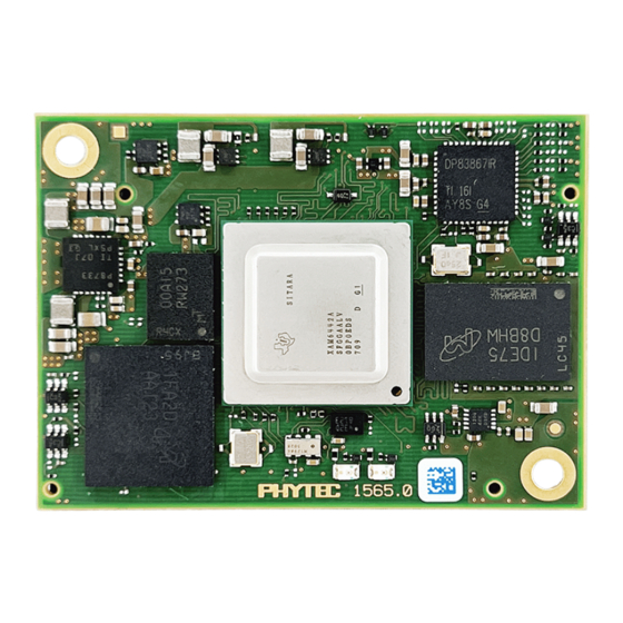
Figure 1. phyCORE-AM64xx SOM The phyCORE-AM64xx belongs to PHYTEC’s phyCORE System on Module family. The phyCORE boards integrate all core elements of a microprocessor system on a single module and are designed in a manner that ensures their easy expansion and embedding in peripheral hardware developments. -
Page 13: Block Diagram
PCM-072/phyCORE-AM64xx System on Module L-860e.A0 4.1 Block Diagram Figure 2. phyCORE-AM64xx Block Diagram © PHYTEC America L.L.C. 2022... -
Page 14: Physical Dimensions
PCM-072/phyCORE-AM64xx System on Module L-860e.A0 4.2 Physical Dimensions Figure 3. phyCORE-AM64xx Dimensions Top View © PHYTEC America L.L.C. 2022... - Page 15 PCM-072/phyCORE-AM64xx System on Module L-860e.A0 Figure 4. phyCORE-AM64xx Dimensions Bottom View Figure 5. phyCORE-AM64xx Dimensions End View © PHYTEC America L.L.C. 2022...
-
Page 16: Connector Alignment For Mating To Carrier Boards
It is recommended to use the following mounting hardware to secure the SOM to a mating carrier board: • 2x M2.5x5mm Female-Female Standoffs 4x M2.5x4mm Screws • 4x M2.5 Washers • Figure 6. Top Down View of Mating Connectors © PHYTEC America L.L.C. 2022... - Page 17 PCM-072/phyCORE-AM64xx System on Module L-860e.A0 Figure 7. Carrier Board Alignment Hole Placement © PHYTEC America L.L.C. 2022...
-
Page 18: Component Placement Diagram
PCM-072/phyCORE-AM64xx System on Module L-860e.A0 4.4 Component Placement Diagram Figure 8. phyCORE-AM64xx Component Placement (processor side) A searchable pdf of the phyCORE-AM64xx component placement (processor side) can be found here: TBD. © PHYTEC America L.L.C. 2022... - Page 19 PCM-072/phyCORE-AM64xx System on Module L-860e.A0 Figure 9. phyCORE-AM64xx Component Placement (connector side) A searchable pdf of the phyCORE-AM64xx component placement (connector side) can be found here: TBD. © PHYTEC America L.L.C. 2022...
-
Page 20: Technical And Electrical Specifications
The phyCORE- AM64xx SOM provides an on-board eMMC, but it is recommended to support another boot source for development and debugging. PHYTEC suggests SD boot for which an example circuit can be seen in section 6.2.2.3 MMC1 Reference Circuit ©... -
Page 21: Solder Jumpers
0 Ω Sets the VDDSHV3 domain to 1.8V NOTE: bold, blue text. Pin 1 is highlighted with an alternate color in Jumper settings show the default position in Figure 10 the solder jumper locations Figure © PHYTEC America L.L.C. 2022... - Page 22 Overheating the board can cause the solder pads to loosen, rendering the module inoperable. Follow the instructions carefully for whatever method of removal is used. CAUTION: If any modifications to the module are performed, regardless of their nature, the manufacturer warranty is voided. © PHYTEC America L.L.C. 2022...
- Page 23 PCM-072/phyCORE-AM64xx System on Module L-860e.A0 Figure 11. Jumper Locations (Connector side) © PHYTEC America L.L.C. 2022...
-
Page 24: Pin Descriptions
These signals should not be driven by any device on the baseboard during reset. The signals that affect the boot configuration are labeled with "BOOTMODE" in the signal name. Details regarding these signals can be found under section 6.3 System Boot Configuration. © PHYTEC America L.L.C. 2022... -
Page 25: Pinout Table
(49.9 pulldown) Ground X_SERDES0_TX0_P Differential AA17 SERDES Differential Transmit Data (positive) X_SERDES0_TX0_N Differential AA16 SERDES Differential Transmit Data (negative) Ground X_SERDES0_RX0_P Differential SERDES Differential Receive Data (positive) X_SERDES0_RX0_N Differential SERDES Differential Receive Data (negative) Ground © PHYTEC America L.L.C. 2022... - Page 26 The voltage level for this signal is configurable for 1.8V or 3.3V via J5. The default voltage level is listed here, but always check the actual jumper setting for the applicable SOM configuration. Refer to section 4.6 Solder Jumpers for details © PHYTEC America L.L.C. 2022...
- Page 27 Ethernet Data A Positive Ground X_CPSW_ETH0_LED_ACTIVITY 3.3V Ethernet LED Activity Signal X_CPSW_ETH0_LED_LINK 3.3V Ethernet LED Link Signal X_CPSW_ETH0_GPIO_0 3.3V Ethernet GPIO 0 X_PRG1_PRU0_GPO8 3.3V PRU Data Output X_PRG1_PRU1_GPO5 3.3V AA13 PRU Data Output Ground X_SPI0_CLK 3.3V SPI Clock © PHYTEC America L.L.C. 2022...
- Page 28 GPMC Data 6 Input/Output X_GPMC0_AD6/BOOTMODE_6 3.3V (100K pullup/pulldown network) Ground GPMC Data 7 Input/Output X_GPMC0_AD7/BOOTMODE_7 3.3V (100K pullup/pulldown network) GPMC Data 8 Input/Output X_GPMC0_AD8/BOOTMODE_8 3.3V (100K pullup/pulldown network) GPMC Data 9 Input/Output X_GPMC0_AD9/BOOTMODE_9 3.3V (100K pullup/pulldown network) © PHYTEC America L.L.C. 2022...
- Page 29 X_CPSW_RGMII2_TX_CTL 3.3V RGMII Transmit Control X_CPSW_RGMII2_TXC 3.3V RGMII Transmit Clock X_PRG1_RGMII1_RD3 3.3V PRU RGMII Receive Data X_PRG1_RGMII1_RD2 3.3V PRU RGMII Receive Data Ground X_PRG1_RGMII1_RD1 3.3V PRU RGMII Receive Data X_PRG1_RGMII1_RD0 3.3V PRU RGMII Receive Data © PHYTEC America L.L.C. 2022...
- Page 30 ADC Analog Input 3 Ground Enhanced Capture (ECAP) Input or Auxiliary PWM X_ECAP0_IN_APWM_OUT 3.3V (APWM) Ouput X_MCAN1_RX 3.3V MCAN Receive Data X_MCAN1_TX 3.3V MCAN Transmit Data X_SPI1_D0 3.3V SPI Data 0 Ground X_SPI1_CS1 3.3V SPI Chip Select 1 © PHYTEC America L.L.C. 2022...
- Page 31 3.3V RGMII Transmit Data 2 X_CPSW_RGMII1_TD3 3.3V AA14 RGMII Transmit Data 3 Ground X_MCU_I2C0_SCL 3.3V MCU_I2C0 Clock X_MCU_I2C0_SDA 3.3V MCU_I2C0 Data RTC Interrupt X_RTC_INT 3.3V (10K pullup) X_RTC_EVI 3.3V RTC Event Input X_PMIC_INT_B PMIC Interrupt © PHYTEC America L.L.C. 2022...
-
Page 32: Thermal Management
5-pin connector that mates with the PHYTEC Carrier board. Finally, the fan is secured to the heatsink with screws. The PHYTEC Carrier Board supplies 5V power to the fan via the DF13-4P-1.25V(75) connector. -
Page 33: Layout Guidelines
Design In Guide sub-sections contain in this document as well as the length of the traces on the SOM. This information can be used to further correct or avoid worsening any SOM trace length mismatches in your own design. © PHYTEC America L.L.C. 2022... -
Page 34: General Signal Routing Guidelines
3.3V voltage source for external circuity. VDD_3V3_OUT goes high VDD_3V3_OUT Deliver 6.6W (2A) B1, B2 after the SOM voltages have stabilized and X_PGOOD goes high. A4, A5, A10, A15, A20, A23, None Ground A26, A29, A35, A40, A45, A50, © PHYTEC America L.L.C. 2022... -
Page 35: Primary System Power (Vin)
An example reference circuit for powering the SOM is shown below. Note that for your own custom carrier board design, a smaller regulator that is closer to the current requirement of your setup can be used in place of the larger regulator shown in the circuit below. © PHYTEC America L.L.C. 2022... - Page 36 Figure 15. External power input overload protection reference circuit Figure 16 is a circuit for measuring the input current to the SOM. It contains: A small resistor (R576) that the current is measured across • © PHYTEC America L.L.C. 2022...
-
Page 37: Backup Power (Vbat)
Cold system Reset X_MCU_RESETz 3.3V Warm Reset of MCU Domain X_RESET_REQz 3.3V Warm Reset of MAIN Domain X_MCU_RESETSTATz 3.3V MCU Domain Reset Status Output X_PORz_OUT 3.3V Cold Reset Status Output X_RESETSTATz 3.3V MAIN Domain Reset Status Output © PHYTEC America L.L.C. 2022... -
Page 38: Power Sequencing
SOM has finished powering up or use VDD_3V3_OUT to power the peripherals. An example of this is shown in the reference circuit below. Figure 17. Carrier board power reference circuit © PHYTEC America L.L.C. 2022... -
Page 39: Safe Shutdown And Sudden Power Loss
Another solution is to have a read-only file system as this would ensure nothing is modified in an unexpected manner in the event of an unexpected shutdown. Figure 18. Example interrupt generation for detecting system power loss © PHYTEC America L.L.C. 2022... -
Page 40: System Memory
The OSPI Flash can be used for a fast boot. Contact our sales team for information on the available OSPI population options: https://PHYTEC.com/contact/ © PHYTEC America L.L.C. 2022... -
Page 41: External Memory Bus
GPMC Address 5 Output X_PRG0_PRU0_GPO18 X_PRG0_PRU0_GPO19 GPMC0_A6 3.3V GPMC Address 6 Output X_CPSW_RGMII2_RD3 X_CPSW_RGMII2_RX_CTL GPMC0_A7 3.3V GPMC Address 7 Output X_PRG0_RGMII2_TD1 X_PRG1_PRU1_GPO5 GPMC0_A8 3.3V GPMC Address 8 Output X_PRG0_RGMII2_TD2 X_CPSW_RGMII2_RXC GPMC0_A9 3.3V GPMC Address 9 Output X_PRG0_RGMII2_TD3 © PHYTEC America L.L.C. 2022... - Page 42 GPMC Data 9 Input/Output (100K pullup/pulldown network) X_GPMC0_AD10/BOOTMODE_10 GPMC0_AD10 3.3V GPMC Data 10 Input/Output (100K pullup/pulldown network) X_GPMC0_AD11/BOOTMODE_11 GPMC0_AD11 3.3V GPMC Data 11 Input/Output (100K pullup/pulldown network) X_GPMC0_AD12/BOOTMODE_12 GPMC0_AD12 3.3V GPMC Data 12 Input/Output (100K pullup/pulldown network) © PHYTEC America L.L.C. 2022...
-
Page 43: Sd/Mmc/Sdio
MMC0 interface is connected to the on-board eMMC. The MMC1 port provides a 4-bit wide data bus that supports SD Host Controller Standard Specification 4.10, SD Physical Layer Specification v3.01, and SDIO Specification v3.00. © PHYTEC America L.L.C. 2022... - Page 44 SD card power needs to be toggled with on board power reset. • Table 16 phyCORE-AM64xx MMC1 Layout Characteristics Signal Name SOM Trace Length (µm) Length Matching (µm) Single Ended Impedance (Ω) X_MMC1_DAT3 33087 X_MMC1_DAT2 28616 X_MMC1_DAT1 33166 12700 X_MMC1_DAT0 32396 X_MMC1_CLK 30210 X_MMC1_CMD 32302 © PHYTEC America L.L.C. 2022...
-
Page 45: System Boot Configuration
BOOTMODE configurations as well as the default configuration on the SOM, which is to boot from eMMC with SD card as a backup. Further BOOTMODE options are discussed in the AM64xx Technical Reference Manual. © PHYTEC America L.L.C. 2022... - Page 46 VDD_3V3_OUT (found on pins B1/B2 at the phyCORE-Connector) or 10kΩ pull-down resistors to override the SOM settings. For startup/verification testing, PHYTEC recommends designing the boot configuration circuit to include a DIP switch. This will make it easy to swap between various boot modes (an example circuit is shown below). This DIP switch can then be de-populated for production.
-
Page 47: Serial Interfaces
The voltage level for this signal is configurable for 1.8V or 3.3V. The default voltage level is listed here, but always check the actual jumper setting for the applicable SOM configuration. Refer to section 4.6 Solder Jumpers for details © PHYTEC America L.L.C. 2022... -
Page 48: Can Reference Circuit
RGMII clock skew. Options such as these can be set via external strapping resistors which are described in the datasheet. The table below lists the default Ethernet PHY strapping configuration; however, these settings can be changed via the © PHYTEC America L.L.C. 2022... -
Page 49: Ethernet Pinout
PHY if necessary. Refer to the DP83867IRRGZ datasheet for further details on these configuration and strapping options (DP83867IRRGZ Datasheet). NOTE: Adjusting strapping options and PHY registers is not necessary when using PHYTEC provided BSPs. Table 19 Ethernet PHY Default Strapping Configuration Strapping Option Default Setting Strapping Signals... - Page 50 PRG1 Management Data IO PRG1_RGMII1_RX_CTL X_PRG1_RGMII1_RX_CTL 3.3V PRG1 RGMII1 Receive Control PRG1_RGMII1_RXC X_ PRG1_RGMII1_RXC 3.3V PRG1 RGMII1 Receive Clock PRG1_RGMII1_RD0 X_ PRG1_RGMII1_RD0 3.3V PRG1 RGMII1 Receive Data 0 PRG1_RGMII1_RD1 X_ PRG1_RGMII1_RD1 3.3V PRG1 RGMII1 Receive Data 1 © PHYTEC America L.L.C. 2022...
- Page 51 RMII1 Receive Data 0 X_CPSW_RGMII1_TD0 X_CPSW_RGMII1_RD1 RMI1_RXD1 3.3V RMII1 Receive Data 1 X_CPSW_RGMII1_TD1 X_CPSW_RGMII1_TD2 RMII1_TXD0 3.3V RMII1 Transmit Data 0 X_CPSW_RGMII1_RD2 X_CPSW_RGMII1_RD3 RMII1_TXD1 3.3V RMII1 Transmit Data 1 X_CPSW_RGMII1_TD3 RMII2_CRS_DV X_CPSW_RGMII2_TD2 3.3V RMII2 Carrier Sense / Data Valid © PHYTEC America L.L.C. 2022...
- Page 52 PRG1_IEP0_EDIO_OUTVALID X_SPI1_CS1 3.3V I/O Outvalid PRU Industrial Ethernet PRG1_IEP0_EDC_LATCH_IN1 X_PRG1_PRU0_GPO7 3.3V Distributed Clock Latch Input PRU Industrial Ethernet PRG1_IEP0_EDC_SYNC_OUT0 X_PRG1_PRU0_GPO19 3.3V Distributed Clock Sync Output PRU Industrial Ethernet PRG1_IEP0_EDC_SYNC_OUT1 X_PRG1_PRU0_GPO17 3.3V Distributed Clock Sync Output © PHYTEC America L.L.C. 2022...
-
Page 53: Ethernet Design In Guide
Place the Ethernet PHY as close as possible to the SOM connector and keep the trace lengths of the RGMII signals as short as possible. • Add a 10kΩ pull-down resistor on any unused input or I/O signal on this interface if it is not connected to a PHY. © PHYTEC America L.L.C. 2022... - Page 54 Carrier Board) + (276860 µm) – (17196 µm) • Receive Clock Length Calculation with Physical Trace Delay: (20030 µm) + (Average total length of control/data signals on Carrier Board) + (276860 µm) – (19732 µm) © PHYTEC America L.L.C. 2022...
- Page 55 PRG0_RGMII2_TXCTL 10482 PRG0_RGMII2_TXD0 10152 PRG0_RGMII2 Transmit PRG0_RGMII2_TXD1 10244 PRG0_RGMII2_TXD2 10263 PRG0_RGMII2_TXD3 10412 PRG0_RGMII2_RXC 10374 AVERAGE_LENGTH(RXCTL, RXD0, RXD1, RXD2, RXD3) + 1.8ns PRG0_RGMII2_RXCTL 10116 2540 µm PRG0_RGMII2 Receive PRG0_RGMII2_RXD0 10340 PRG0_RGMII2_RXD1 9922 PRG0_RGMII2_RXD2 10274 PRG0_RGMII2_RXD3 10265 © PHYTEC America L.L.C. 2022...
- Page 56 28627 PRG1_RGMII2_RXD1 28431 PRG1_RGMII2_RXD2 31957 PRG1_RGMII2_RXD3 30883 These signals are not length matched on the SOM and the differences in length matching will need to be accounted for in your own custom carrier board design. © PHYTEC America L.L.C. 2022...
- Page 57 For industrial ethernet peripheral (IEP) the following two changes need to be accounted for: • Connect ETH_LINK to LED0 on the Ethernet PHY • Connect ETH_ERR to either LED1 on the Ethernet PHY or pull down to ground. © PHYTEC America L.L.C. 2022...
-
Page 58: Ethernet Reference Circuits
PRG0_RGMII1 signals to an Ethernet PHY are shown below. Figure 22. RJ45 Reference Schematic The circuit consists of: • An Ethernet Jack • Two TVS diode arrays for ESD protection • Two voltage networks to manage the Ethernet LEDs in the jack © PHYTEC America L.L.C. 2022... - Page 59 PCM-072/phyCORE-AM64xx System on Module L-860e.A0 © PHYTEC America L.L.C. 2022...
- Page 60 PCM-072/phyCORE-AM64xx System on Module L-860e.A0 © PHYTEC America L.L.C. 2022...
-
Page 61: Fsi
Ethernet PHYs you plan to populate, this may or may not be necessary). 7.3 FSI The phyCORE-AM64xx SOM provides two Fast Serial Interface Transmitter (FSI_TX) cores and six Fast Serial Interface Receiver (FSI_RX) cores. The FSI cores can be used to communicate with an FSI-enabled device. © PHYTEC America L.L.C. 2022... -
Page 62: Fsi Pinout
The voltage level for this signal is configurable for 1.8V or 3.3V. The default voltage level is listed here, but always check the actual jumper setting for the applicable SOM configuration. Refer to section 4.6 Solder Jumpers for details This signal should not be driven during reset. More information can be found in section 6.3 System Boot Configuration © PHYTEC America L.L.C. 2022... -
Page 63: I 2 C
PCIe shares its SERDES signals with USB 3.1 and only one can be used at a time (both systems can be populated on a custom CB as long as the SERDES signals are run through a multiplexer). © PHYTEC America L.L.C. 2022... -
Page 64: Pcie Pinout
X_SERDES0_REFCLK0_N. The external clock must be a high-quality, low-jitter differential 100MHz clock source compliant to the PCIe REFCLK AC specifications. We recommend using the PI6C557-03 clock generator, which is implemented on the PHYTEC carrier board. A PCIe reference circuit is shown in section 7.5.3 PCIe Reference Circuits. - Page 65 PCM-072/phyCORE-AM64xx System on Module L-860e.A0 Figure 24. PCIe Reference Schematics © PHYTEC America L.L.C. 2022...
-
Page 66: Spi
SPI3 Data In SPI4_CLK X_UART0_CTS 3.3V SPI4 Clock SPI4_CS0 X_UART1_RTS 3.3V SPI4 Chip Select 0 SPI4_CS1 X_MCAN0_TX 3.3V SPI4 Chip Select 1 SPI4_CS2 X_MCAN0_RX 3.3V SPI4 Chip Select 2 SPI4_CS3 X_ECAP0_IN_APWM_OUT 3.3V SPI4 Chip Select 3 © PHYTEC America L.L.C. 2022... -
Page 67: Uart
UART0 is the default console and as such PHYTEC recommends bringing out UART0 for console access. More information on using it as a debug console is provided in section 10.3... - Page 68 X_PRG0_PRU0_GPO19 X_GPMC0_AD4/BOOTMODE_4 (100K pullup/pulldown network) X_PRG0_RGMII1_RX_CTL UART3_TXD 3.3V UART3 Transmit Data X_UART1_RTS X_MMC1_DAT0 X_PRG0_PRU0_GPO18 X_GPMC0_AD10/BOOTMODE_10 (100K pullup/pulldown network) UART4_CTSN 3.3V UART4 Clear to Send X_PRG0_RGMII2_RXC X_PRG0_RGMII1_RXC X_PRG0_PRU0_GPO19 UART4_RTSN 3.3V UART4 Request to Send X_PRG0_PRU1_GPO8 X_GPMC0_CLK © PHYTEC America L.L.C. 2022...
- Page 69 X_PRG0_RGMII2_RD3 X_GPMC0_BE0n_CLE X_I2C0_SDA UART6_RTSN 3.3V UART6 Request to Send (2.2K pullup) X_PRG0_PRU1_GPO5 X_GPMC0_AD14/BOOTMODE_14 (100K pullup/pulldown network) X_SPI0_CS1 UART6_RXD 3.3V UART6 Receive Data X_PRG0_RGMII2_TD3 X_CPSW_RGMII1_RD2 X_GPMC0_AD15/BOOTMODE_15 (100K pullup/pulldown network) UART6_TXD 3.3V UART6 Transmit Data X_SPI1_CS1 X_PRG0_RGMII2_RX_CTL © PHYTEC America L.L.C. 2022...
-
Page 70: Usb
Differential USB3 Super Speed 3 Transmit Data Negative X_SERDES0_TX0_P Differential USB3 Super Speed 3 Transmit Data Positive X_SERDES0_RX0_N Differential USB3 Super Speed 3 Receive Data Negative X_SERDES0_RX0_P Differential USB3 Super Speed 3 Receive Data Positive © PHYTEC America L.L.C. 2022... -
Page 71: Usb Design In Considerations
An example of this in layout is shown in Figure 25 The right image shows a filter, and the left image shows the ground plane cutout beneath it. Figure 25. Layout example of a ground cutout. © PHYTEC America L.L.C. 2022... -
Page 72: Usb Reference Circuits
7.8.3 USB Reference Circuits Example reference circuits for connecting the SERDES differential signals and USB0 signals to a HUB and then connecting the HUB to a USB 3.1 connector are shown below. Figure 26. USB-HUB Reference Schematic © PHYTEC America L.L.C. 2022... -
Page 73: Control Interfaces
Enhanced Capture (ECAP) Input or ECAP1_IN_APWM_OUT X_MCAN1_TX 3.3V Auxiliary PWM (APWM) Output Enhanced Capture (ECAP) Input or ECAP2_IN_APWM_OUT X_MCAN1_RX 3.3V Auxiliary PWM (APWM) Output PRU-ICSSG Enhanced Capture (ECAP) X_CPSW_MDC PRG0_ECAP0_IN_APWM_OUT 3.3V Input or Auxiliary PWM (APWM) (1.5K pullup) Output © PHYTEC America L.L.C. 2022... -
Page 74: Enhanced Pulse-Width Modulation
Two PWM outputs that can be used as either: o Two independent PWM outputs with single-edge operation o Two independent PWM outputs with dual-edge symmetric operation o One independent PWM output with dual-edge asymmetric operation © PHYTEC America L.L.C. 2022... -
Page 75: Epwm Pinout
3.3V EHRPWM Output A EHRPWM5_B X_GPMC0_WAIT0 3.3V EHRPWM Output B X_GPMC0_CSn3 EHRPWM_TZn_IN5 3.3V EHRPWM Trip Zone Input 5 (active low) X_GPMC0_WAIT1 X_SPI1_CS0 EHRPWM6_A 3.3V EHRPWM Output A X_GPMC0_ WPn EHRPWM6_B X_SPI1_D1 3.3V EHRPWM Output B © PHYTEC America L.L.C. 2022... -
Page 76: Enhanced Quadrature Encoder Pulse
EQEP Quadrature Input A X_PRG0_RGMII2_RD0 X_UART0_TX EQEP0_B X_GPMC0_ DIR 3.3V EQEP Quadrature Input B X_PRG0_RGMII2_RD1 X_UART0_RTS X_GPMC0_CSn1 EQEP0_I 3.3V EQEP Index X__PRG0_RGMII2_TD2 X_CPSW_RGMII1_RD1 X_UART0_CTS EQEP0_S X_GPMC0_CSn0 3.3V EQEP Strobe X_PRG0_RGMII2_RD2 EQEP1_A X_UART1_RX 3.3V EQEP Quadrature Input A © PHYTEC America L.L.C. 2022... -
Page 77: Peripheral Interfaces
ADC0_AIN2 X_ADC2 1.8V ADC Analog In 2 ADC0_AIN3 X_ADC3 1.8V ADC Analog In 3 ADC0_AIN4 X_ADC4 1.8V ADC Analog In 4 ADC0_AIN5 X_ADC5 1.8V ADC Analog In 5 ADC0_AIN6 X_ADC6 1.8V ADC Analog In 6 © PHYTEC America L.L.C. 2022... -
Page 78: Cpts
X_ECAP0_IN_APWM_OUT 3.3V CPTS Time Stamp Generator Bit 0 SYNC1_OUT X_EXT_REFCLK1 3.3V CPTS Time Stamp Generator Bit 1 SYNC2_OUT X_MCAN0_TX 3.3V CPTS Time Stamp Generator Bit 2 SYNC3_OUT X_MCAN0_RX 3.3V CPTS Time Stamp Generator Bit 3 © PHYTEC America L.L.C. 2022... -
Page 79: Gpio
GPIOs to check for pull-up and pull-down resistors, connected devices, etc. CAUTION: The majority of the GPIO pins can be either 1.8V or 3.3V depending on the jumper settings. Take care when using these signals and consider the voltage levels. © PHYTEC America L.L.C. 2022... -
Page 80: Gpio Pinout
X_GPMC0_WAIT1 3.3V None GPIO0_39 X_GPMC0_WPn 3.3V None GPIO0_40 X_GPMC0_DIR 3.3V None GPIO0_41 X_GPMC0_CSn0 3.3V None GPIO0_42 X_GPMC0_CSn1 3.3V None GPIO0_43 X_GPMC0_CSn2 3.3V None GPIO0_44 X_GPMC0_CSn3 3.3V None GPIO0_45 X_PRG1_RGMII1_RD0 3.3V None GPIO0_46 X_PRG1_RGMII1_RD1 3.3V None © PHYTEC America L.L.C. 2022... - Page 81 The voltage level for this signal is configurable for 1.8V or 3.3V. The default voltage level is listed here, but always check the actual jumper setting for the applicable SOM configuration. Refer to section 4.6 Solder Jumpers for details © PHYTEC America L.L.C. 2022...
- Page 82 X_CPSW_RGMII1_RD3 3.3V DNU if on-board ETH PHY is populated GPIO1_38 X_CPSW_MDIO 3.3V 1.5K pullup GPIO1_39 X_CPSW_MDC 3.3V 1.5K pullup GPIO1_40 X_PRG0_MDIO0_MDIO 3.3V None GPIO1_41 X_PRG0_MDIO0_MDC 3.3V None GPIO1_43 X_SPI0_CS1 3.3V None GPIO1_44 X_SPI0_CLK 3.3V None © PHYTEC America L.L.C. 2022...
- Page 83 Table 48 MCU_GPIO0 Accessibility at phyCORE-Connector Processor X1 Pin #(s) SOM Signal(s) Type Level Internal SOM Usage Signal MCU_GPIO0_0 X_MCU_UART0_RTS 3.3V None MCU_GPIO0_1 X_MCU_UART0_CTS 3.3V None MCU_GPIO0_2 X_MCU_UART0_TX 3.3V None MCU_GPIO0_3 X_MCU_UART0_RX 3.3V None © PHYTEC America L.L.C. 2022...
- Page 84 X_PRG0_RGMII1_TD0 3.3V None PRG0_PRU0_GPI12/GPO12 X_PRG0_RGMII1_TD1 3.3V None PRG0_PRU0_GPI13/GPO13 X_PRG0_RGMII1_TD2 3.3V None PRG0_PRU0_GPI14/GPO14 X_PRG0_RGMII1_TD3 3.3V None PRG0_PRU0_GPI15/GPO15 X_PRG0_RGMII1_TX_CTL 3.3V None PRG0_PRU0_GPI16/GPO16 X_PRG0_RGMII1_TXC 3.3V None PRG0_PRU0_GPI17/GPO17 X_PRG0_PRU0_GPO17 3.3V None PRG0_PRU0_GPI18/GPO18 X_PRG0_PRU0_GPO18 3.3V None PRG0_PRU0_GPI19/GPO19 X_PRG0_PRU0_GPO19 3.3V None © PHYTEC America L.L.C. 2022...
- Page 85 X_PRG1_PRU0_GPO7 3.3V None PRG1_PRU0_GPI8/GPO8 X_PRG1_PRU0_GPO8 3.3V None DNU if on-board ETH PHY is PRG1_PRU0_GPI9/GPO9 X_CPSW_RGMII1_TX_CTL 3.3V populated DNU if on-board ETH PHY is PRG1_PRU0_GPI10/GPO10 X_CPSW_RGMII1_TXC 3.3V populated PRG1_PRU0_GPI11/GPO11 X_PRG1_RGMII1_TD0 3.3V None PRG1_PRU0_GPI12/GPO12 X_PRG1_RGMII1_TD1 3.3V None © PHYTEC America L.L.C. 2022...
-
Page 86: Timer
9.4.1 Timer Pinout Table 53 Timer Signals Processor Signal X1 Pin #(s) SOM Signal(s) Type Level Description X_I2C1_SCL TIMER_IO0 3.3V Timer Inputs and Outputs X_MMC1_DAT3 TIMER_IO1 X_I2C1_SDA 3.3V Timer Inputs and Outputs © PHYTEC America L.L.C. 2022... -
Page 87: Debug Interfaces
The phyCORE-AM64xx SOM is equipped with a JTAG interface for downloading program code into the internal RAM or for debugging programs currently executing. The JTAG interface is accessible via the phyCORE-Connector and provides seven standard IEEE1149.6 JTAG signals. © PHYTEC America L.L.C. 2022... -
Page 88: Jtag Pinout
Connectors and Pinout. Figure 28. JTAG Reference Schematic 10.2 TRACE (TRC) The phyCORE-AM64xx SOM is equipped with a TRACE (TRC) module that can be used to record operation of the ROM code and debug unexpected occurrences. © PHYTEC America L.L.C. 2022... -
Page 89: Trc Pinout
The voltage level for this signal is configurable for 1.8V or 3.3V. The default voltage level is listed here, but always check the actual jumper setting for the applicable SOM configuration. Refer to section 4.6 Solder Jumpers for details This signal should not be driven during reset. More information can be found in section 6.3 System Boot Configuration © PHYTEC America L.L.C. 2022... -
Page 90: Uart0
The phyCORE-AM64xx SOM can also be communicated with using UART0 for downloading program code into the internal RAM or for debugging programs currently executing. UART0 is the default console and as such PHYTEC recommends bringing out UART0 for console access. The UART0 interface is accessible via the phyCORE-Connector. - Page 91 A TVS diode array for ESD protection • A micro-USB connector • A simpler design that just brings out the bare minimum UART signals for use with FTDI USB adapter cables is shown below. Figure 30. Simple UART0 Reference Schematic © PHYTEC America L.L.C. 2022...
-
Page 92: System Interfaces
The voltage level for this signal is configurable for 1.8V or 3.3V. The default voltage level is listed here, but always check the actual jumper setting for the applicable SOM configuration. Refer to section 4.6 Solder Jumpers for details © PHYTEC America L.L.C. 2022... -
Page 93: Integrating And Handling The Phycore-Am64Xx
12.3 In-Field Updates It is important that your system is designed so that firmware can be updated remotely in case there are issues "in the field." PHYTEC recommends choosing at least one or more of the following design features: •... -
Page 94: Product Change Management
Instead, PHYTEC manages this at the SOM-level. PHYTEC ensures continued availability of pin- and function-compatible SOMs and SBCs, further minimizing maintenance costs and risks. This pro- active product lifecycle management (PLM) policy has enabled deployment of the same PHYTEC SOM in designs for over twenty years. -
Page 95: Additional Information
PHYTEC System on Modules (SOM) and Single Board Computers (SBC) are designed as subcomponents for integration in electrical devices. Combined with PHYTEC Carrier Boards, PHYTEC SOMs can be used as dedicated Evaluation Boards (i.e.: for use as a test and prototype platform for hardware/software development) in laboratory environments. - Page 96 - are reserved. No reproduction may occur without the express written consent from PHYTEC. The information in this document has been carefully checked and is as reliable as possible. However, PHYTEC assumes no responsibility for any inaccuracies. PHYTEC neither gives any guarantee nor accepts any liability whatsoever for consequential damages resulting from the use of this manual or its associated product.
-
Page 97: Revision History
PCM-072/phyCORE-AM64xx System on Module L-860e.A0 14 Revision History Table 59 Document Revision History Date Version Number Changes in this Manual 2022/06/02 L-860e.A0 Preliminary Release © PHYTEC America L.L.C. 2022...
Need help?
Do you have a question about the phyCORE-AM64 Series and is the answer not in the manual?
Questions and answers