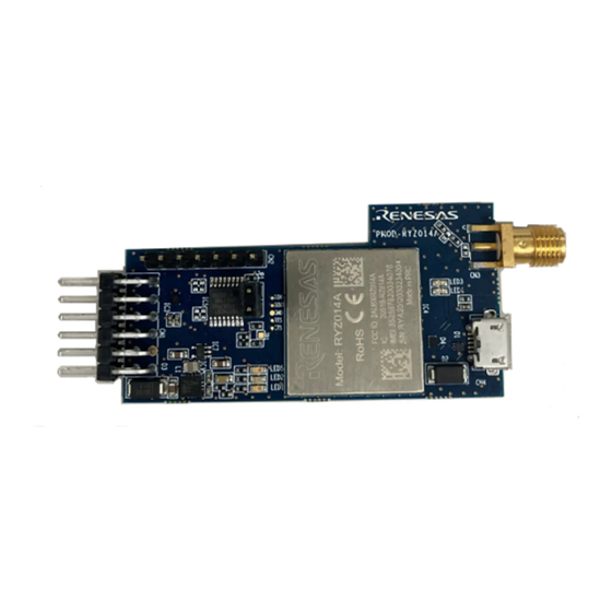
Renesas RYZ014A Datasheet
Lte category m1 module
Hide thumbs
Also See for RYZ014A:
- User manual (39 pages) ,
- Integration manual (32 pages) ,
- Quick start manual (20 pages)
Table of Contents
Advertisement
Quick Links
Datasheet
RYZ014A
LTE Category M1 Module
Description
The RYZ014A is a complete certified LTE Category M1 module including base-band, RF and memory, for
the design of connected machine-to-machine devices, and other Internet-of-Things devices with embedded
LTE connectivity. This document provides technical information about RYZ014A LGA module.
This document is intended for engineers who are developing User Equipment (UE) for LTE systems.
Functions
Renesas RYZ014A module includes Monarch SQN3330 Cat-M1 baseband, a complete dual band RF front
end, memory and required circuitry to meet 3GPP E-UTRA (Long Term Evolution - LTE, Release 13) Cat-M1
UE specifications.
For more information on the core technology specifications see the section References on page 32. The term
RYZ014A module refers to the hardware and the associated embedded software.
Figure 1. RYZ014A Block Diagram
Table 1 provides detail on general features of the RYZ014A.
Table 2 provides detail for the LTE-related features of the RYZ014. The module's ECCN and part number
are detailed in the section ECCN and Part Number on page 14.
R19DS0111EU0102 Rev.1.02
Page 1 of 33
Mar.29.22
Advertisement
Table of Contents

Related Manuals for Renesas RYZ014A


Summary of Contents for Renesas RYZ014A
- Page 1 LTE Category M1 Module Description The RYZ014A is a complete certified LTE Category M1 module including base-band, RF and memory, for the design of connected machine-to-machine devices, and other Internet-of-Things devices with embedded LTE connectivity. This document provides technical information about RYZ014A LGA module.
- Page 2 RYZ014A LTE Category M1 Module Datasheet Table 1. General Features Feature Description • General interfaces JTAG • I2C (reserved) • USIM • SPI (reserved) • GPIO • UART (x3, including one reserved) • RING • WAKE • • 32 kHz...
-
Page 3: Pin Description
RYZ014A LTE Category M1 Module Datasheet Feature Description • PDCP Ciphering and deciphering: NULL, AES, SNOW 3G • Integrity and protection: AES, SNOW 3G • MIB and new SIB1-BR • Intra and inter-frequency cell reselection • Intra-frequency connected mode mobility •... - Page 4 RYZ014A LTE Category M1 Module Datasheet Pad# Pad Name Direction Default Function Description Alternate Function Capability Description (Contact Renesas Support Team for detail on persistent AT Commands availability) GPIO27/CTS2 UART2/CTS (OUT). It is recommended to pull-up this pad with the application host processor supply...
- Page 5 RYZ014A LTE Category M1 Module Datasheet Pad# Pad Name Direction Default Function Description Alternate Function Capability Description (Contact Renesas Support Team for detail on persistent AT Commands availability) All GND pads shall be connected to the same copper. GNSS_WAKEUP Reserved, do not use. Do Not Connect All GND pads shall be connected to the same copper.
- Page 6 RYZ014A LTE Category M1 Module Datasheet Pad# Pad Name Direction Default Function Description Alternate Function Capability Description (Contact Renesas Support Team for detail on persistent AT Commands availability) Analog Analog Digital Converter TXD2 UART2/TXD (IN), if not used should be connected to a Test Point.
- Page 7 RYZ014A LTE Category M1 Module Datasheet Pad# Pad Name Direction Default Function Description Alternate Function Capability Description (Contact Renesas Support Team for detail on persistent AT Commands availability) GPIO17/CTS1 GPIO17: Reserved, no function. UART1/CTS (OUT) CTS1 active low. No Flow control by default.
- Page 8 RYZ014A LTE Category M1 Module Datasheet Pad# Pad Name Direction Default Function Description Alternate Function Capability Description (Contact Renesas Support Team for detail on persistent AT Commands availability) GNSS_VCC3 Reserved, do not use. Do Not Connect GPIO29/32KHZ_CLK_OUT Reserved for future use. Do not connect.
- Page 9 RYZ014A LTE Category M1 Module Datasheet Pad# Pad Name Pad Type Drive State Power (mA) drive toggling @reset Group strength freq (all that will modes) be used (MHz) (mA) SIM_IO SIM_VC BIDIR In, PU SIM_VCC VBAT1 Power High-Z, PD GNSS_TXD3...
- Page 10 RYZ014A LTE Category M1 Module Datasheet Pad# Pad Name Pad Type Drive State Power (mA) drive toggling @reset Group strength freq (all that will modes) be used (MHz) (mA) SPI_SDO BIDIR In, PU RTS0 VBAT1 BIDIR_WAKE In, HiZ CTS0 BIDIR 6.25...
- Page 11 OEM integrators only. Installation/Integration OEM integrators must follow Renesas’ installation instructions to provide for and benefit from FCC compliant module integrations and must abide especially by the following: The maximum antenna gain values (accounting for cable attenuation) to comply with the FCC maximum ERP/EIRP limits and with RF Exposure rules: •...
- Page 12 RYZ014A LTE Category M1 Module Datasheet End-product Labelling • FCC-ID The module's FCC-ID must either be visible from the exterior of the host product (e.g. per window) or per electronic display, or shall be displayed on an additional exterior label per the following or similar string: contains FCC-ID: 2AU6XRZ014A •...
-
Page 13: Industry Canada Statement
RYZ014A LTE Category M1 Module Datasheet Industry Canada Statement This device complies with ISED’s licence exempt RSSs. Operation is subject to the following two conditions: (1) This device may not cause harmful interference, and (2) this device must accept any interference received, including interference that may cause undesired operation. -
Page 14: Physical Characteristics
D200247003). Terminal devices with built-in modules need to be certified according to security standards. Declaration of Conformity for EU RE Directive Hereby, Renesas Electronics America Inc. declares that the radio equipment type RYZ014A is in compliance with Directive 2014/53/EU. The equipment must be powered by a PS1 source in compliance with the 62368-1 standard. - Page 15 They shall not be used to power external IC or parts that require permanent supply. RYZ014A Power Tree Figure 2 provides a representation of the power tree of the RYZ014A. All current values are maximum RMS current. Figure 2. RYZ014A Power Tree R19DS0111EU0102 Rev.1.02...
- Page 16 RYZ014A LTE Category M1 Module Datasheet Power Supplies Environment Figure 3 illustrates the connections between the RF front-end power supplies of the RYZ014A. Figure 3. RYZ014A LTE RF Front-End Power Supplies Diagram Environmental Operating Conditions Temperature • RF compliant: -30°C to +85°C (measured on board thermistor) •...
- Page 17 RYZ014A LTE Category M1 Module Datasheet I/O Characteristics The voltage and current characteristics of the various IO pads of the RYZ014A versus IO bank supply voltage are illustrated in the tables below. Caution: Note that the V values in the tables below do not apply to GPIOs configured in open drain mode.
- Page 18 RYZ014A LTE Category M1 Module Datasheet Parameter Drive Strength Min. Nom. Max. Unit ±10 µA Tri-state Output Leakage Current @ VO=1.8V or 0V Input Capacitance kOhm Pull-up Resistor kOhm Pull-down Resistor 2 mA Low Level Output Current at V (max)
- Page 19 Important: If the ADC input is directly connected to an external device which doesn’t drive 0V when the RYZ014A is in Sleeping Mode, then an external analog switch (such as FET) must be connected to ADC input pin to prevent any current leakage in PMU sleeping state.
- Page 20 RYZ014A LTE Category M1 Module Datasheet Item Test Conditions Standard Result 3 samples for each discharge level. Conduct up to 4kV the discharge tests on the upper cover and all bottom pads of the samples. Temperature Cycle 10 temperature cycles from -40°C to +85°C;...
- Page 21 RYZ014A LTE Category M1 Module Datasheet Module Footprint Figure 4. Module Top and Side View and Dimensions Note: Figure 5 is a view of the pads seen on the module, and Figure 6 represents the footprint of the module on the PCB. Pad #1 is located on the top right of the module in Figure 5 and will be soldered on the top left area of the PCB footprint on Figure 6.
- Page 22 RYZ014A LTE Category M1 Module Datasheet Figure 6. Module Detailed Bottom View and Dimensions (PCB View) Marking Information Figure 7. RYZ014A Marking Description R19DS0111EU0102 Rev.1.02 Page 22 of 33 Mar.29.22...
- Page 23 RYZ014A LTE Category M1 Module Datasheet Table 13. Marking Details Symbol Description Renesas Logo RYZ014A Product Name RoHS logo FCC ID: 2AU6XRZ014A IC: 20519-RZ014A IMEI: XXXXXXXXXXXXXXX (15 digits) S/N: RYAYYMMDDPPPPXXX (16 digits) RYA: is immovable (3 digits) YYMMDD: Manufacturing Date (YY: Year, MM: Month, DD: Date) PPPP: Panel Counter (4 digits 0001-9999);...
-
Page 24: Storage Conditions
5. If baking is required, refer to IPC/FEDEC J-STD-033 for bake procedure. Note: Level and body temperature are defined by IPC/JEDEC J-STD-020. Mounting Considerations The RYZ014A can support up to 3 reflows with 250°C maximum. R19DS0111EU0102 Rev.1.02 Page 24 of 33... - Page 25 Ramp-down rate -4.99 °C/s Signals and Pins RYZ014A Pinout The signals and all the related details are listed in the MS-Excel companion file delivered together with the present document in a PDF portfolio. The pads listed in Table 16 are connected to ground.
- Page 26 • Port RXD on the Host Application receives data from the module’s RXD signal line. Figure 10. UART0, UART1 and UART2 Signals Convention and Flow Control Note: Voltage level compatibility between the Host Application’s UART signals and the RYZ014A UART signals shall be verified. Use a level shifter if necessary.
- Page 27 Important: RYZ014A UART0 is configured with hardware flow control (RTS0, CTS0). During the boot cycle, it is mandatory that the Application Host connected to UART0 implements hardware flow control on its UART, because the RYZ014A will send SYSSTART URC. Not complying with this requirement can prevent the module to boot.
- Page 28 Important: The RYZ014A module is provided with an internal RTC whose supply is VBAT1. As a consequence, VBAT1 should not be removed, in order to keep RTC active. The RYZ014A will automatically enter in low-power mode. RYZ014A can be woken from low power mode by external sources through: •...
- Page 29 RYZ014A LTE Category M1 Module Datasheet Figure 13 shows a simplified diagram of the Digital bi-directional IOs in Sleep Mode or active mode. Figure 13. Digital Bi-Directional IOs in Sleep Mode or Active Mode • Behavior in Deep Sleep Mode In Deep Sleep Mode the Digital bi-directional IOs are completely powered Off.
- Page 30 RYZ014A LTE Category M1 Module Datasheet • Behavior in Deep Sleep Mode. Note: The PMU bi-directional wake IOs output buffer is disabled in Deep Sleep Mode. Figure 15 shows a simplified diagram of the PMU bi-directional wake IOs in Deep Sleep Mode.
- Page 31 RYZ014A LTE Category M1 Module Datasheet Acronym Definition Downlink DPLL Digital Phase-Locked Loop ECCN Export Control Classification Number Evolved Packet System Electro-Static discharge ETSI European Telecommunications Standard Institute Federal Communications Commission (USA) Ground GPIO General Purpose Input Output Human Body Model (ESD tests)
- Page 32 RYZ014A LTE Category M1 Module Datasheet Acronym Definition User Equipment UICC Universal integrated circuit card (SIM) Uplink XTAL Crystal References 1. Core technology specifications: • 3GPP E-UTRA 21 series Release 13 (EPS) • 3GPP E-UTRA 22 series Release 13 (IMEI) •...
-
Page 33: Revision History
RYZ014A LTE Category M1 Module Datasheet Revision History Description Rev. Date Page Summary 1.00 Apr.13.21 Initial release. 1.01 Jul.21.21 Added Japan radio/terminal equipment based on type certification 1.02 Mar.29.22 2, 3, 19 Updated Table 1, General Features, Table 2, LTE Features, added Table 12, Reliability Test Results. -
Page 34: General Precautions In The Handling Of Microprocessing Unit And Microcontroller Unit Products
Unit Products The following usage notes are applicable to all Microprocessing unit and Microcontroller unit products from Renesas. For detailed usage notes on the products covered by this document, refer to the relevant sections of the document as well as any technical updates that have been issued for the products. -
Page 35: Corporate Headquarters
Renesas Electronics disclaims any and all liability for any damages or losses incurred by you or any third parties arising from the use of any Renesas Electronics product that is inconsistent with any Renesas Electronics data sheet, user’s manual or other Renesas Electronics document.
Need help?
Do you have a question about the RYZ014A and is the answer not in the manual?
Questions and answers